AI: From ‘Accelerator’ to ‘Paradigm Reconstructor’ in Metaphotonics
 10/23 2026
 469

Abstract: Traditional metaphotonics design relies heavily on repetitive trial-and-error methods, with massive arrays of nanorods creating immense computational burdens.
AI is not merely accelerating simulations; it is reshaping the entire design paradigm. Diffusion models, large language models (LLMs), and AI agents are shifting the focus from human-driven trial-and-error to AI-generated designs, revolutionizing the field.
The most frustrating aspect of metasurface design is not the slow simulations themselves, but the internal friction caused by repeated iterative parameter tuning. With AI, designers can finally automate the process of "defining the desired response first, then determining the structure," bringing unprecedented ease and efficiency.
This article explores upstream design tools, which differ significantly from mass-producing optical waveguides. A single metalens may contain millions of nanorods, each requiring precise geometric design to function correctly.
Traditionally, engineers rely on experience to build a structure, run simulations to verify it, and adjust parameters if the results are unsatisfactory. A single simulation can take tens of minutes on an ordinary computer, and a complete design cycle can span weeks or even months.
Searching for the optimal design within such a vast parameter space pushes the limits of human intuition and traditional computational methods. AI is changing this landscape—not by simply accelerating existing processes, but by introducing a fundamentally new design approach.
The Traditional Design Deadlock—Why Does Metaphotonics 'Stall'?
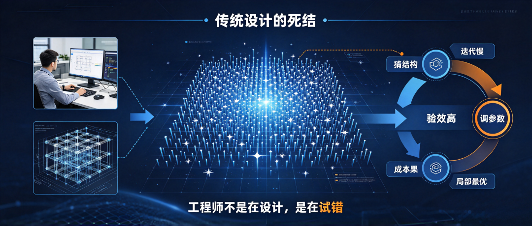
The design dilemma in metasurfaces arises from the asymmetry between the "forward problem" and the "inverse problem." The forward problem (predicting the optical response given a structure) is relatively straightforward but still requires solving Maxwell's equations, with each simulation taking tens of minutes on an ordinary computer.
The inverse problem (deducing the structure given an optical response) is far more challenging. The same optical response may correspond to countless possible structures. Traditional inverse design methods reformulate the problem as an optimization task, relying on iterative algorithms that repeatedly call simulations.
Each iteration involves "guessing" a structure and "verifying" its performance, leading to slow convergence, high computational costs, and a tendency to get stuck in local optima. In essence, engineers are not truly "designing" but rather engaging in a prolonged process of trial and error.
Diffusion Models: Stop Iterating, Just Draw It Out
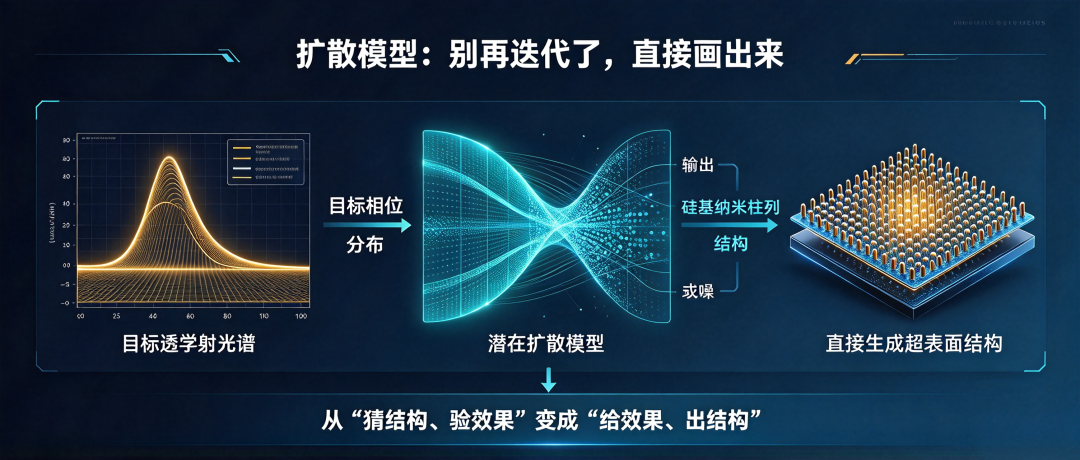
Tsinghua University's AIGP framework represents a landmark case in paradigm reconstruction. The research team proposed an inverse design framework based on latent diffusion models, enabling direct mapping from optical properties to subwavelength structures.
Its core innovation lies in transforming the design problem from an "optimization problem" into a "generation problem."
Engineers simply input the desired optical properties—such as a target transmission spectrum or phase distribution—and AIGP generates the corresponding metasurface structure directly, akin to "drawing a picture." This approach entirely eliminates the need for iterative optimization.
The team validated 64 structural color meta-atoms on a silicon-based platform, successfully encoding a sunflower image onto a chip and achieving "generation as manufacturing."
For an ideal long-pass filter response that is physically unrealizable, AIGP provided a near-optimal solution in seconds. The design logic has been completely flipped—from "guessing the structure and verifying the effect" to "defining the effect and generating the structure."
LLMs: Translating 'I Need a Phase Distribution' into a Structure
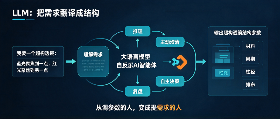
While diffusion models solve the problem of "structure generation," large language models (LLMs) address "requirement translation."
A research team at Penn State introduced LLMs into the metasurface design process, allowing engineers to describe requirements in natural language. The LLMs then directly predict how the metasurface will affect light, streamlining the design workflow.
Their method validated prediction accuracy on a dataset of 45,000 randomly generated metasurface designs while eliminating the time-consuming process of customizing neural networks for each specific metasurface.
Stanford University's MetaChat framework takes this a step further by introducing the concept of "self-reflective AI agents."
AI can not only design metasurfaces but also "look back" at its previous designs after each round, autonomously deciding the next optimal action without relying on predefined templates.
In tests, MetaChat designed a metalens that focuses blue light to one point and red light to another. The AI automatically configured the structural parameters with assistance from material experts, actively asking users questions to clarify requirements during the process.
The engineer's role is shifting from "parameter tuner" to "requirement proposer," at least during the generative design phase.
Nanjing's Platform: The Value Lies in Calibration and Quality Inspection, Not Chatting
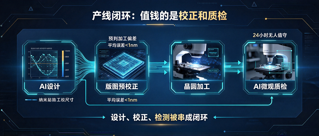
Beyond academic breakthroughs, industrial-side changes better illustrate the depth of this paradigm reconstruction. In July 2026, Nanjing Tech released the MetaODA metasurface AI integrated computing platform.
This platform attempts to streamline the entire process from design to inspection, with Nanjing Tech being one of the few successful cases. Key features include:
- AI-automated design: Compressing a 10-hour design task into 30 minutes, boosting R&D efficiency nearly 20-fold.
- AI-intelligent layout correction: Neural network correction models predict processing deviations in advance, controlling the average error between drawings and physical objects to within 1 nanometer.
- AI fully automated microscopic quality inspection: Automatically identifying nanostructures at each calibration location, supporting 24-hour unattended operation.
- Wafer fully automated optical inspection: Increasing inspection efficiency from 400 wafers per hour to 1,500.
According to public data and manufacturer disclosures, with this platform, Nanjing Tech's disclosed delivery rhythm is "1 day for optical solution output, 2 weeks for sample trial production, 4 weeks for mass delivery," though this data is not third-party audited. Its self-owned production line discloses a stable monthly output of millions of metalenses.
Metalenz's first-generation meta-optical components have shipped in the hundreds of millions, while Shenzhen Metalenz discloses near-infrared metalens production capacity in the range of 1-2 million units (subject to official latest disclosures).
AI is not just "assisting" mass production but redefining production speed—but only if yield keeps up.
What Does This Mean for AR Optics?

Returning to the AR optical waveguide track, the fusion of AI and metaphotonics has two major implications.
First, it significantly improves design iteration speed.
AR glasses' optical solutions must simultaneously satisfy multiple constraints, such as field of view (FOV), light efficiency, thinness, and dispersion control. Under traditional design processes, each iteration takes weeks.
AI generative design compresses iteration cycles to days or even hours, making "rapid trial-and-error, rapid convergence" possible.
Second, it enables the emergence of end-to-end systems.
A review by the Korea University team points out that the fusion of AI and metaphotonics is spawning "end-to-end" systems—where physical hardware (metasurfaces) and software (AI algorithms) are designed synchronously. This allows cameras to self-correct defects and optical systems to adapt to environmental changes.
For AR glasses, this means the optical module is no longer a "fixed-parameter hardware" but an "intelligent optical system" capable of sensing the environment and dynamically adjusting.
AI's transformation of metaphotonics is not about making old processes faster but making them unnecessary.
From diffusion models' "generative design" to LLMs' "natural language design" to MetaODA's "design-correction-inspection closed loop"—metaphotonics is moving from "human trial-and-error" to "AI generation."
For AR optics, iteration cycles shift from years to months, from months to weeks—but only if etching and thin-film processes keep up; otherwise, what AI designs cannot be manufactured on production lines.
Interactive Topic: In your optical design work, have AI tools already started changing your workflow? Or do you still rely on traditional simulations and manual parameter tuning? Welcome to share your experiences in the comments.
— AR Andy | Focused on the optical waveguide and AR microdisplay track, deeply dissecting the underlying logic of the optics industry
[Risk Disclaimer] This article is for industry popularization of science purposes; academic cases and industrial data are sourced from public literature and manufacturer releases. Mass production of meta-devices remains constrained by engineering factors such as etching, thin-film processes, and yield. AI design outputs still require process validation and cannot be directly equated with finished products. Shipment volumes, production capacities, and delivery rhythms mentioned are subject to each manufacturer's official latest disclosures; AI-generated designs ≠ mass production-ready without production line yield verification.
-
![]()
Will Doubao Mobile Trigger a New Round of 'Soul Theory' Debate?
-
![]()
Doubao Phone: Will It Spark a Fresh Wave of 'Soul Theory' Controversy?
-
![]()
When AI Creates Problems but No One Is Held Accountable: It Gave the Police a False Tip
-
![]()
From Doubao Mobile Phone to OPPO’s Partnership with Manus, and the Gradual Rise of Startups like Jieyue Xingchen: Who’s Riding the Wave of Opportunity?
-
![]()
Audi in Negotiations with Huawei: Developing Next-Gen A8 for China Using Huawei’s Platform, with Plans for Multiple New Models | Mirror Pro
-
![]()
People Trapped in Algorithms
-
![]()
Musk’s Computing Power Venture Recoups Investment Within a Year, Meta’s Muse Faces Uncertain Rollout Timeline
-
![]()
AI: From ‘Accelerator’ to ‘Paradigm Reconstructor’ in Metaphotonics