The Other Side of the 'First Year of Mass Production' of Optical Waveguides: Has Capacity Been Built Up and Yield Kept Up?
 09/28 2026
 389
389

Abstract: The year 2026 has been defined by the industry as the first year of mass production for optical waveguides, with various companies achieving million-piece-level production capacities, making it seem like the sector has fully entered a large-scale era.
However, capacity expansion does not equate to stable mass production. The industry's true core barriers have shifted from 'whether it can be done' to 'whether it can be done stably and with high yield.'
The three major bottlenecks—materials, processes, and inspection—are interconnected. Breakthroughs in isolated technologies cannot solve mass production challenges; full-link system capabilities are the core competitiveness in the second half of the optical waveguide sector.
The year 2026 is definitely the first year of mass production for optical waveguides. Capacity planning across the sector is more aggressive than ever before.
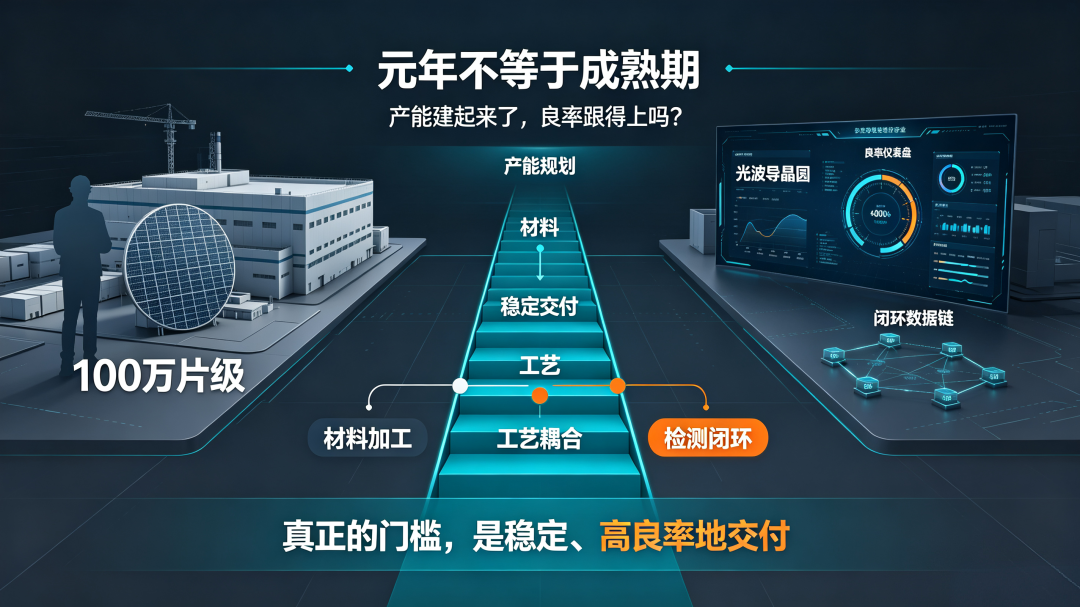
ZhiGe Technology is striving to deliver million-piece-level SRG waveguides, AAC Technologies has stably broken through an 80% yield rate in its SRG production line, Nika Optics has officially launched its million-piece-level VHG production line, and Lipai Optical Crystal has upgraded its annual production capacity to the million-unit level.
Suddenly, optical waveguides have completely moved beyond the small-batch sampling stage and are fully charging toward large-scale implementation. However, there is a truth in the industry that is easily overlooked: capacity can be rapidly scaled up, but yield cannot be quickly improved.
As ZhiGe Technology CEO Meng Xiangfeng said: The large-scale mass production of new-generation waveguides like polarization volume holograms (PVH) cannot be achieved through standardized equipment procurement.
The true logic of mass production involves working backward from material R&D to define process windows, then redefining non-standard automated equipment based on process requirements, and finally continuously adjusting parameters through massive production data. This is not just a pain point for a single company but a systemic bottleneck that the entire optical waveguide supply chain must face.
01 Material Bottleneck: SiC's Hard and Brittle Nature Sets a Baseline for Mass Production Yield
The first major hurdle in optical waveguide mass production has never been optical design but material processing.
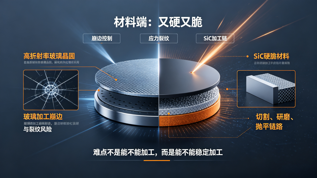
Even processing mature high-refractive-index glass, long recognized as a tough challenge in the industry, presents significant difficulties. High-refractive-index glass is hard and brittle, making traditional mechanical cutting prone to edge chipping and cracks, which not only affect appearance but also directly damage the optical effective area and create stress risks.
According to Huagong Laser industry data: Reducing edge chipping by 1μm significantly lowers optical loss and cracking risk. Currently, the industry's top level can only control edge chipping to ≤10μm.
The new-generation silicon carbide (SiC) material is even more difficult to process than glass. SiC's ultra-high hardness and extreme brittleness result in much lower yields throughout the cutting, grinding, and polishing processes compared to traditional glass materials.
Although Tanyu Advanced has completed technological breakthroughs in 12-inch SiC substrate production, substrate mass production does not equal stable lens processing. From raw material substrates to usable optical lenses, a mature processing chain has not yet been fully established.
The ultimate bottleneck at the material end has never been 'whether it can be processed' but whether it can be processed in large quantities over the long term, stably, and with high yield.
02 Process Bottleneck: Deeply Coupled Parameters and Chain-Reaction Defects
After overcoming material challenges, more hidden and fatal difficulties lie in precise process control.
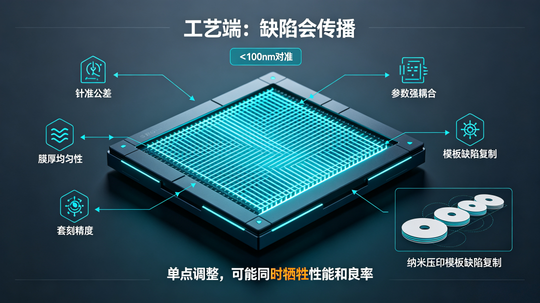
Manufacturing high-end SRG diffractive optical waveguides for full-color and large FOV applications requires extremely stringent precision.
In large-area substrate processing scenarios, alignment and overlay accuracy often need to be controlled at the <100nm level, while precisely managing grating depth, tilt angle, film thickness uniformity, and overall defect density.
Most critically: All process parameters are deeply coupled—a change in one affects all others.
Optimizing a single parameter often compromises another optical performance, making it impossible to achieve a balance between yield and performance through isolated adjustments.
Additionally, defect propagation caused by nanoimprint lithography is an invisible killer of large-scale mass production.
Tiny organic defects introduced during the template stage, if not promptly intercepted, will continuously spread and amplify with each imprinting replication, turning local minor flaws into systemic yield accidents across entire batches.
This is why the industry repeatedly emphasizes 'full-link deep coupling': Optical waveguide mass production has never been about purchasing a set of equipment and setting up a production line; it is a systemic project highly bound to materials, processes, and equipment.
03 Inspection Bottleneck: Sub-Nanometer Precision Determines Mass Production Closed-Loop Capability
Being able to process is just the foundation; being able to inspect accurately is the core of stable mass production.
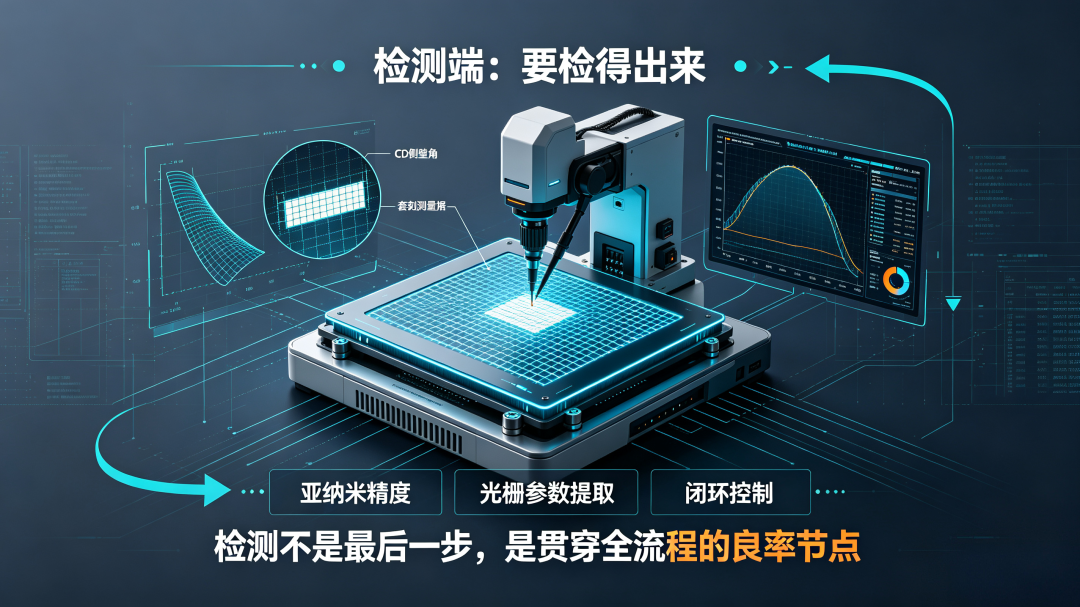
Manufacturing high-end full-color SRG optical waveguides now requires sub-nanometer-level inspection standards.
Leading metrology equipment and demonstration-level indicators on advanced production lines have reached industry-top standards: Relying on RCWA rigorous coupled-wave analysis technology, the industry can simultaneously and accurately extract core parameters such as grating depth, critical dimensions, and sidewall angles; high-precision image overlay measurement achieves ultra-low measurement uncertainty of 0.83nm in the X direction and 0.92nm in the Y direction.
Meanwhile, for metal film metrology on Cr and Al hard mask layers, wafer-level uniformity can be controlled within 2%, with repeatability precision below 0.15%.
In true mass production logic, inspection is never the final finishing process but a quality closed-loop node run through ing material, process, molding, and module assembly.
Only by connecting, series connection ing, and reviewing inspection data from each process step can mass production yield be stabilized at the root.
04 Industry Breakthrough: Moving Beyond Isolated Breakthroughs to Embrace Full-Link Coupling
Across the entire optical waveguide sector, there are no shortcuts to future mass production breakthroughs.
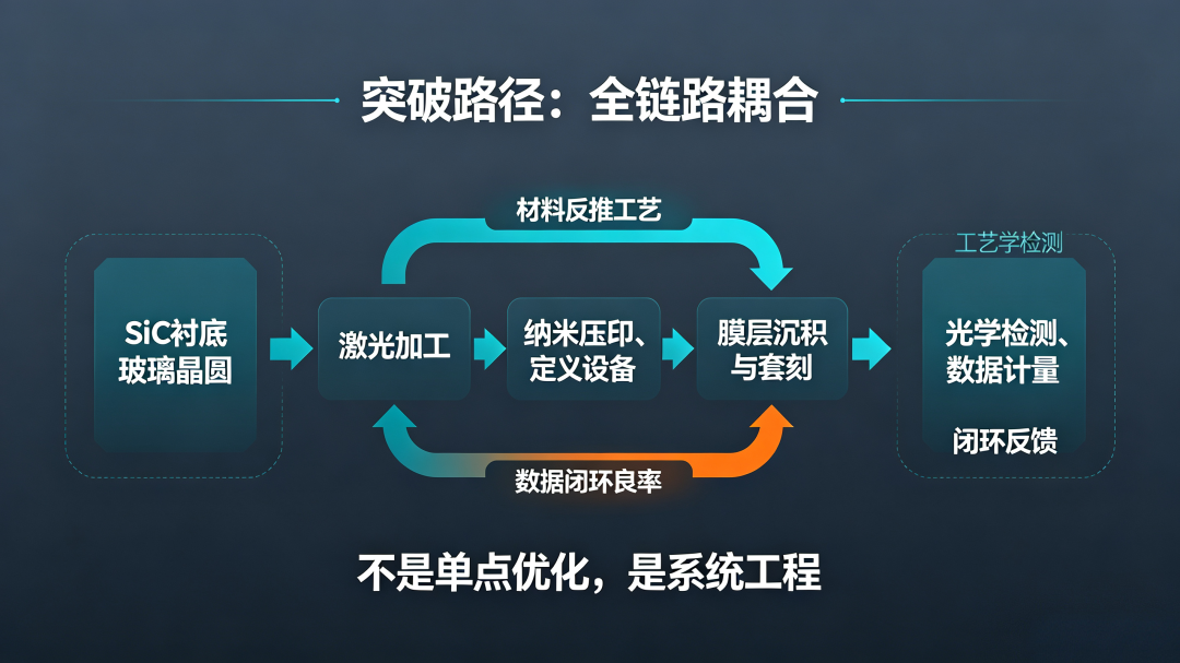
Isolated material upgrades, single-process optimizations, or individual equipment iterations cannot fully resolve mass production bottlenecks. The only solution is deep coupling across materials, processes, and inspection.
On the material side, San'an Optoelectronics' 6/8-inch SiC optical wafers have passed certification from international leading clients, with 12-inch products undergoing simultaneous sampling verification; Goertek Olley has established 12-inch transparent substrate and DUV lithography capabilities, continuously strengthening the upstream wafer process foundation.
On the process side, intelligent laser processing lines have begun large-scale implementation.
Huagong Laser's second-generation AR optical waveguide intelligent production line has achieved fully automated processing of 8-12-inch glass wafers while reserving expansion capabilities for SiC material processing to accommodate future material iteration needs.
On the inspection side, the industry is widely promoting a 'inspection-first' mass production approach: Moving defect screening and precision verification to the wafer stage to intercept defective products early and establishing a implementable yield closed-loop control system through full-process data series connection .
However, it must be clarified: Breakthroughs in material substrates, iterations in laser processing equipment, and implementation of high-precision metrology solutions represent isolated capabilities of upstream materials, process equipment, and inspection equipment, respectively. They do not mean that any single optical waveguide manufacturer has independently achieved a complete mass production closed loop covering 'materials-processes-inspection.'
What the industry truly lacks today is the systemic architecture capability to uniformly translate upstream material parameters, mid-stream process windows, and downstream inspection data into a stable yield and controllable cost mass production system.
05 Yield Data Reveals True Industry Generation Gaps
Currently published yield data in the industry clearly shows tiered gaps.
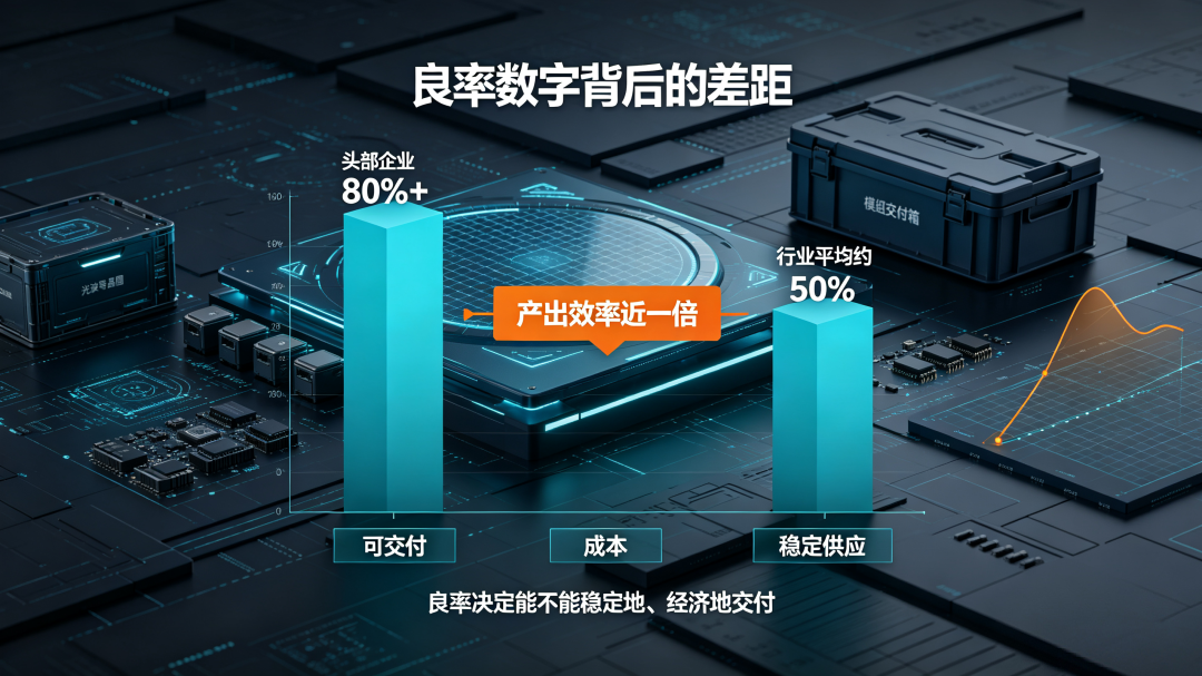
AAC Technologies has disclosed that its SRG production line maintains a stable mass production yield above 80%, ZhiGe Technology has publicly announced a first-pass yield exceeding 85%, with yields reaching 90% for projects with leading clients.
A commonly cited benchmark in industry exchanges is that the overall average mass production yield across the sector still hovers around 50%; a quantifiable mass production generation gap has opened between leading companies and small-to-medium-sized players.
This data gap represents not just minor technical differences but generation gaps in mass production and commercialization capabilities.
For the same production line investment, an 80% yield versus a 50% yield nearly doubles the effective output, directly determining product cost, delivery speed, and market competitiveness.
This is also why leading companies can commercialize solutions like 'single-layer full-color, over 50% weight reduction': Only sufficiently high yields can support stable, economical large-scale delivery.
Final Thoughts: The first year of mass production for optical waveguides in 2026 is not a numerical competition in production capacity scale but a real engineering battle.
Material processing, process coupling, and inspection closed loops—none of these three hurdles are glamorous, but each can derail mass production plans.
There is no magic to mass production; it simply involves refining material parameters, process windows, inspection data, yield, and cost into a replicable system through hundreds or thousands of trial production rounds.
Moving from 'can be done in the lab' to 'can be stably manufactured on the production line' presents engineering implementation challenges far greater than theoretical technological breakthroughs.
The optical waveguide companies that will succeed in the future will compete not on production capacity numbers announced at press conferences but on who first translates 'materials-processes-inspection' into a unified yield language and precipitate s it into a scalable, deliverable, and cost-reducible systemic mass production capability.
Interactive Topic: Among the three major bottlenecks in optical waveguide mass production—material processing, process control, and inspection precision—which do you believe is the hardest to fully overcome? Welcome to leave a comment and exchange ideas.
—— AR Andy | Focusing on the optical waveguide and AR microdisplay sectors, deeply dissecting the underlying logic of the optics industry
[Risk Disclaimer] This article is compiled based on publicly available industry information and industrial research, intended solely for discussion of industry perspectives and does not constitute investment or procurement advice. Production capacity and yield data from various companies are subject to the latest official disclosures.
-
![]()
Honor Magic9 Pro Max Review: Imaging Gets More Exciting, Agent System Impresses
-
What questions does the Third Pioneering Venture of Volkswagen in China Need to Answer with ID. UNIQ 09?
-
Why is Geely introducing Zhichong now, and what stage has Geely's new energy strategy reached?
-
![]()
Fuel Vehicle Sales Slump and New Energy Gaps Present Limited Growth Avenues for Joint Ventures
-
![]()
How to Calculate MTF from a Slanted Edge? A Three-Step Derivation from ESF to the Curve
-
![]()
The Other Side of the 'First Year of Mass Production' of Optical Waveguides: Has Capacity Been Built Up and Yield Kept Up?
-
![]()
Huawei Set to Unveil '10x Zoom Module Camera'! Patent Visuals Unveiled: Boasts Built-in CMOS
-
![]()
Silicon Carbide Optical Waveguides: From 'Performance Option' to 'Mass Production Element'