"Geken, an ambitious 'doer'"
![]() 08/29 2024
08/29 2024
![]() 491
491
"CMOS image sensors have long been well-known in the industry. Since 2007, CMOS image sensors surpassed CCD image sensors in market share for the first time, marking the beginning of their golden era."
Among the fluctuations in the global CIS market, international giants like Sony and Samsung have long dominated, consistently ranking among the top two in sales. However, upon closer inspection of global CIS shipment data, Geken's name stands out prominently.
01
"Breaking Through" in CIS
In 2003, engineer Zhao Lixin returned to China to start his own business. At that time, China's semiconductor industry was just emerging, and few local companies were present in the domestic image sensor market. Later, with the aspiration to "let the world see China's innovation," Geken was founded.
Rich people rely on money, while poor people rely on hard work.
Unlike Weir Corporation , which relied on acquisitions to expand, Geken took a different path: relying on independent research and development, leveraging technological and price advantages to carve out a niche.
At that time, there was a business development need at SMIC, and the two sides quickly reached an agreement. By 2006, Geken and SMIC had jointly developed an innovative CMOS image sensor core process. Due to its cost advantages and strong products, Geken achieved revenue of $8 million and began to establish itself domestically. Since then, Geken has continuously focused on CMOS image sensors and LCD display driver chips, continuously innovating.
In 2017, Geken successfully achieved mass production of a 1.12um large-base 13MP image sensor, breaking the technological blockade imposed by overseas manufacturers. By 2019, it had completed the research and development of a 16MP CMOS chip.
Geken astutely capitalized on the global smartphone boom, precisely targeting the mid-to-low-end market. With the accelerating trend of multi-camera smartphones, Geken, as a supplier to major Android smartphone brands, has seized this era-given opportunity and continued to thrive.
By 2021, Geken delivered impressive results. Its CMOS image sensor shipments reached 1.9 billion units, ranking first globally; sales revenue reached $900 million, ranking fourth globally. From obscurity to prominence, Geken persevered through "innovation."
The global CMOS image sensor market is constantly evolving, and Geken has its unique advantages. Qiao Jingxuan, Vice President of Geken, said, "The competitive landscape of global CMOS image sensors should be viewed from three dimensions: first, brand advantage supported by technology; second, unique sales channels; third, self-owned factories after depreciation. From the first dimension, after 20 years of development, Geken has been accumulating competitiveness in core technologies. At the same time, Geken has also entered the Fab-Lite model, enabling more technological innovations to be implemented. From the remaining two dimensions, although Geken started later compared to overseas giants, with the vigorous development of the consumer electronics market, Geken's unique advantages have allowed it to catch up quickly. Therefore, Geken can compete with overseas competitors in all three aspects."
"Innovation" is deeply ingrained in Geken's DNA. In addition to process R&D and product design innovations, Geken also has "innovations" in its business model.
In mid-2023, Geken's Lingang factory officially commenced mass production, marking the successful transformation of Geken into the Fab-Lite model. Fab-Lite is a business model that falls between the Fabless model and the IDM model, combining self-built factories and outsourcing in wafer manufacturing, packaging, and testing.
Generally speaking, most chip design companies listed on the A-share market adopt the Fabless model. Domestic CIS company Weir Corporation also adopts the Fabless model. However, Sony and Samsung, the other two major players in the CIS field, adopt the IDM model.
Regarding why Geken chose the Fab-Lite model, Qiao Jingxuan analyzed its two major advantages. On the one hand, Fab-Lite can smooth out production capacity fluctuations. A significant characteristic of the semiconductor industry is its cyclical nature, which includes product inventory cycles and equipment investment cycles. When these two cycles overlap, the semiconductor industry exhibits very pronounced cyclical features. Fab-Lite acts as a "reservoir" for production capacity, ramping up production during tight capacity periods and focusing on R&D during loose capacity periods. On the other hand, and more importantly, the Fab-Lite model can better support Geken's technological breakthroughs in process and device R&D, enhancing the core competitiveness of its products. The Lingang factory's process development is characterized by "big strides," focusing on more forward-looking and groundbreaking innovations, primarily targeting high-end, high-margin products in fields such as mobile phones, automobiles, and smart cities, emphasizing "high performance." Currently, numerous technological and process R&D initiatives are underway at the Lingang factory.
It is understood that in the first half of the year, Geken's Lingang factory successfully achieved mass production of 8MP and 13MP products, and small-scale production of 50MP products. In the first half of 2024, the Lingang factory generated revenue of RMB 1.277 billion, a year-on-year increase of 468.15%, with a significant narrowing of net profit losses compared to the same period last year.
02
Why Geken?
A few days ago, Geken released its financial report for the first half of 2024, revealing that in the first half of this year, Geken achieved operating revenue of RMB 2.79 billion, an increase of 42.94% year-on-year; net profit attributable to shareholders was RMB 77.49 million, turning around from a loss to a profit year-on-year.

Sales of Various Product Lines in the First Half of 2024
By product, Geken's revenue from CMOS chips for mobile phones accounted for 56.06% of total revenue in the first half of this year. This proportion has gradually increased from the end of the first half of 2023 to the end of 2023 and then to the end of June this year. At the same time, the average price per chip has also increased from RMB 2.65 per chip in the first half of last year to RMB 3.42 per chip. In terms of CMOS image sensors for non-mobile phone applications, sales revenue also increased by 29.74% year-on-year in the first half of the year.
Geken's rapid growth is rooted in technology and talent.
Qiao Jingxuan stated that the technological characteristics of mobile phone CIS can be summarized as "two highs and one low." "Two highs" refer to high pixel count and high dynamic range. Currently, sensors in mobile phone main cameras have evolved from 12MP to 48MP, 50MP, and even 100MP and 200MP products, making high pixel count a trend in mobile phone main camera CIS development. High dynamic range refers to the requirement for a wider dynamic range. Currently, 10-bit dynamic range is mainstream in mobile phone CIS, with future advancements expected to reach 12-bit and beyond for better imaging results. "One low" refers to low power consumption. Due to the small size and heat dissipation constraints of mobile phones, mobile phone CIS inherently requires low power consumption to address these issues, which are exacerbated by high pixel count and high dynamic range requirements.
Currently, in the mobile phone CIS field, Geken has a significant advantage in high pixel integration technology, having achieved mass production of 13MP to 32MP products, with various 50MP products also in small-scale production. Additionally, in the first half of this year, Geken successfully mass-produced the high-performance second-generation 32MP image sensor GC32E2, equipped with single-frame high dynamic range DAG HDR technology. This product, which offers rich bright and dark details and artifact-free images at lower power consumption, has been initially launched on the OPPO Reno12 overseas edition and will continue to be promoted among brand customers.
The non-mobile phone sector also has its unique technological characteristics, as described by Qiao Jingxuan as "two lows and one high." "One high" refers to high dynamic range, which is particularly important in the TOB market due to storage and transmission constraints, making high dynamic range a consistent demand across various scenarios. "Two lows" refer to low power consumption and low noise. Currently, image sensors are competing fiercely in power consumption, as it significantly affects imaging quality, and the demand for low power consumption persists. Meanwhile, low noise is crucial in scenarios such as surveillance, aerial photography, and night photography.
In the field of non-mobile phone CMOS image sensors, Geken continues to promote 4MP and 8MP products. Currently, Geken's 4MP product shipments are continuously increasing, and 8MP products have successfully achieved mass production shipments. In the first half of the year, Geken successfully developed the new-generation 4MP product GC4103, equipped with infrared-enhanced NIR and supporting pre-recording for Always-on functionality, offering lower power consumption and enhanced "night vision" capabilities compared to previous generations.
Qiao Jingxuan stated, "While mobile phone CIS and non-mobile phone CIS differ in product characteristics, there is also some technological overlap, and Geken has achieved collaborative development and advancement in both fields."
Furthermore, Geken participates in the cultivation of Chinese chip talent through various forms, such as continuously supporting the China Graduate Electronics Design Contest. When asked about the initial motivation behind supporting the contest, Qiao Jingxuan reminisced, "When we first supported the contest around 2017, Chinese people were relatively unfamiliar with chips and integrated circuits. The industry did not fully understand academia, and academia was unaware of industry issues. Professor Zhou Zucheng, the founder of the contest, approached us, hoping to bridge the gap between industry and academia through the contest. Geken's motivation was simple: someone needed to do it, and if no one else was willing, we would step up. Little did we know that this endeavor would span eight years. Through this contest platform, we have gained a lot, including deeper interactions with universities and the recruitment of more outstanding talent."
03
Future Blueprint
From humble beginnings in a makeshift workshop to becoming a global industry giant with top shipments, Geken has persevered through "innovation."
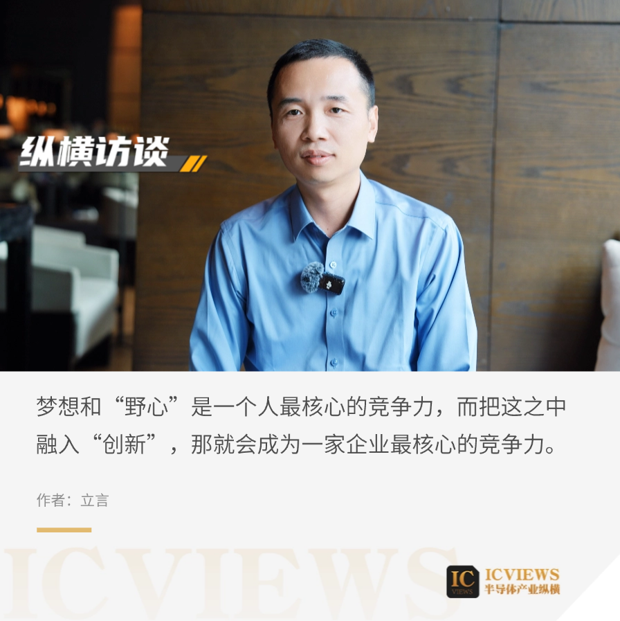
When asked about the impact of emerging technologies on Geken, Qiao Jingxuan said that technologies such as AI, IoT, and big data are preparing humanity for a smarter future. Imaging will be a crucial component of this future smart society. Specifically, in terms of hardware, image sensors capture images, while display driver chips display them, making them two critical links in imaging. Geken has consistently focused on imaging to build its core competencies. Dreams and "ambition" are an individual's core competitiveness, and when integrated with "innovation," they become a company's core competitiveness. As Qiao Jingxuan firmly believes, "We strive to become a respected world-class provider of comprehensive imaging solutions." Geken is steadfastly taking Chinese innovation to the world, one step at a time.
