Among HBF, HMC, and Two Other Major Memory Types, Who Can Rival HBM?
 01/05 2026
 723
723
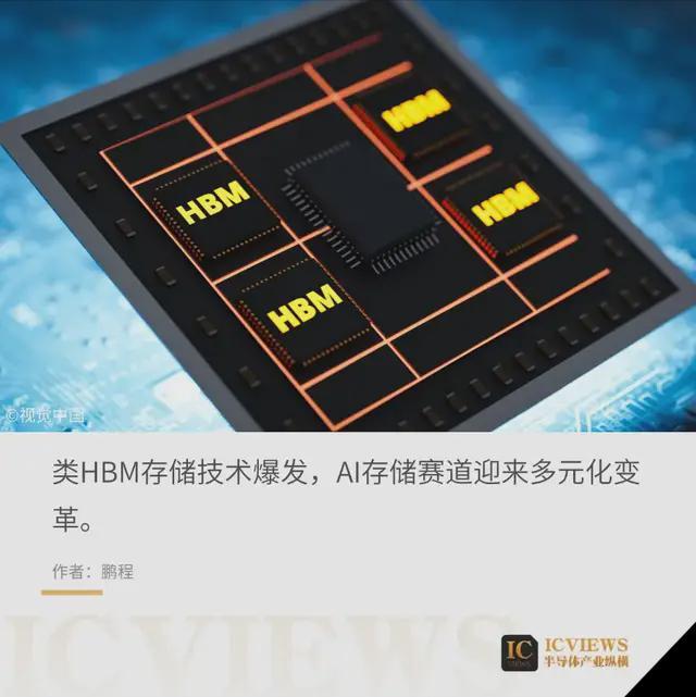
As the core component of current AI accelerator GPUs, High Bandwidth Memory (HBM) offers crucial support for AI training and inference. Its vertically stacked thin DRAM chip architecture and ultra-high data bandwidth have made it a cornerstone of the AI computing power surge.
However, HBM has two notable drawbacks. Firstly, its cost remains significantly higher, being an order of magnitude more expensive than standard DDR memory. Secondly, its capacity growth is constrained by the technical bottleneck of DRAM memory density scaling. Even NVIDIA's Blackwell GPU, equipped with eight 24GB HBM3e chip stacks (totaling 192GB), struggles to meet the massive memory demands driven by explosive model scaling, extended context lengths, and AI video generation. In this context, developing lower-cost, higher-capacity alternative technologies has become an industry consensus, accelerating the rise of HBM-like technologies and propelling the AI memory sector into an era of diversified competition.
01
SPHBM4: Standard Packaging Redefines HBM's Application Scope
The JEDEC Solid State Technology Association recently announced the near-completion of the SPHBM4 standard ("SP" stands for "Standard Package"). As a derivative technology of HBM4, SPHBM4 retains the same DRAM chip and stacking architecture as HBM4, maintaining equivalent single-stack capacity. The key difference lies in the optimized design of the Interface Base Die, which can be directly mounted on standard organic substrates instead of the silicon interposers used in traditional HBM4. This fundamentally alters HBM's physical integration approach.
In terms of performance parameters, HBM4 stacks feature a 2048-bit interface, doubling the previous 1024-bit interface—the largest breakthrough since HBM's debut in 2015. In contrast, SPHBM4 reduces the single-stack interface bit width to 512 bits. It achieves data transfer rates comparable to HBM4 by increasing operating frequency and adopting 4:1 serialization technology, while relaxing the bump pitch requirements for organic substrates and reducing packaging complexity. More importantly, the organic substrate wiring enables SPHBM4 to support longer SoC-to-memory channel distances, allowing further total memory capacity expansion through increased stack counts and providing new solutions for high-capacity demand scenarios.
It is crucial to emphasize that SPHBM4 is not a "low-cost version of HBM" or a "downgraded alternative." Its core memory performance aligns with HBM4, with its primary value lying in breaking HBM's application limitations of "high cost and AI accelerator exclusivity." With standardization, HBM technology is expected to expand into CPUs, network chips, cloud ASICs, and other scenarios, driving substantial market scale expansion. For the three major memory giants—SK Hynix, Samsung Electronics, and Micron—SPHBM4's compatibility with existing HBM DRAM chips enables them to maintain high-end technological competitiveness while capturing new market demands. Additionally, the alleviation of packaging constraints will transform large-scale stable supply capabilities into new competitive advantages.
02
HBF: High Bandwidth Flash Ushers in a New Era of Capacity Competition
HBF (High Bandwidth Flash) features a structure similar to HBM's stacked DRAM chips but is fabricated by stacking NAND flash memory. Compared to DRAM, NAND flash offers significantly higher capacity density, with NAND capacity reaching up to 10 times that of DRAM in the same footprint—a characteristic perfectly suited for AI scenarios' urgent demand for large-capacity storage. HBF achieves multi-layer NAND chip vertical stacking through Through-Silicon Via (TSV) technology, employing advanced 3D stacking architectures and chip-to-wafer bonding techniques to construct a densely interconnected memory structure.
In balancing performance and capacity, HBF demonstrates outstanding advantages. Each package can stack up to 16 NAND chips, supporting parallel access to multiple NAND arrays with bandwidth ranging from 1.6TB/s to 3.2TB/s, on par with HBM3. Simultaneously, HBF achieves significantly higher capacity than HBM at similar costs. With single-stack capacity reaching up to 512GB and total capacity of 4TB with eight stacks, it offers 8-16 times the capacity of HBM. Furthermore, HBF breaks traditional NAND design by implementing independently accessible memory sub-arrays, surpassing conventional multi-plane methods and further enhancing parallel access capabilities and throughput.
However, constrained by NAND flash's inherent characteristics, HBF exhibits higher latency than DRAM, making it more suitable for read-intensive AI inference tasks rather than latency-sensitive applications. Despite not yet in mass production, HBF has attracted industry giants to enter the field. In February 2025, SanDisk launched the first HBF prototype and established a technical advisory board. In August of the same year, SanDisk and SK Hynix signed a memorandum of understanding to advance specification standardization and ecosystem development, planning to deliver engineering samples in the second half of 2026 and achieve commercialization in early 2027. Samsung Electronics has initiated conceptual design for its proprietary HBF products. Kioxia showcased a prototype with 5TB per module capacity and 64GB/s bandwidth at the 2025 Flash Memory Summit. Domestic manufacturers are also entering the HBF market, with products aligning with AI's "cloud-edge collaboration" trend, providing high-bandwidth, large-capacity support for edge AI inference and facilitating AI terminal application deployment.
03
HBS Memory: A Low-Cost, High-Performance Solution for Terminal AI
While HBM dominates data center AI scenarios, SK Hynix is developing High Bandwidth Storage (HBS) technology for AI computing demands in smartphones, tablets, and other terminal devices, aiming to overcome terminal AI's memory performance bottlenecks. HBS employs Vertical Fan-Out (VFO) packaging technology, vertically stacking up to 16 layers of DRAM and NAND chips. By directly connecting chips with straight wires instead of traditional curved wire connections, it significantly shortens electrical signal transmission paths (less than 1/4 of traditional memory), effectively reducing signal loss and latency while supporting more I/O channels.
At the performance level, VFO packaging technology improves HBS's energy efficiency by 4.9%, reduces packaging thickness by 27%, and increases heat dissipation by only 1.4%, achieving an optimized balance between performance and form factor. At the cost level, HBS eliminates the need for Through-Silicon Via (TSV) processes, as chip manufacturing does not require drilling, significantly improving yield rates and reducing production costs, facilitating adoption by terminal device manufacturers. Although SK Hynix has not announced a specific mass production timeline for HBS, this technology is expected to bring more powerful local AI processing capabilities to terminal devices, driving AI application proliferation from the cloud to terminals and reshaping the terminal intelligence ecosystem.
04
HMC Memory: A Classic Technology's Differentiated Comeback
Developed jointly by Micron and Intel, HMC (Hybrid Memory Cube) initially aimed to address DDR3's bandwidth bottleneck. Its core structure connects four DRAM dies to a logic control chip at the stack's base layer using 3D TSV technology. Compared to HBM, HMC eliminates the interposer, directly interconnecting through an ABF substrate, resulting in a simpler structure and lower latency. However, its bandwidth capability is generally weaker than HBM's, and it imposes higher requirements on substrate trace density and system-level design capabilities.
After HBM's introduction and adoption as a JEDEC industry standard, HMC gradually became marginalized, leading Micron to announce its discontinuation in 2018 and shift focus to HBM. However, as AI memory demands for cost and differentiation intensify, HMC has re-entered industry consideration. From cost and power consumption perspectives, HMC avoids the yield pressures associated with HBM's interposer and advanced packaging, resulting in lower manufacturing costs and stronger supply chain controllability. Although its peak bandwidth and energy efficiency density fall short of HBM's, the trade-offs of relatively higher power density and increased system design complexity can be offset through differentiated optimization in specific scenarios. In the future, HMC is expected to find its niche in customized AI systems, becoming a crucial option for deep integration of computing power, memory, and advanced packaging.
Today, the AI industry is moving away from the single HBM-dominated era and entering a new phase of diversified technological routes. Whether it's NVIDIA's promotion of new DRAM modules like SOCAMM, 3D NAND vertical stacking architectures represented by HBF, or differentiated technologies such as SPHBM4, HBS, and HMC, the core competition in AI memory has shifted from single-technology performance comparisons to comprehensive evaluations of cost, mass production capabilities, and system-level overall efficiency.
The future market landscape will feature clear differentiated roles. HBM will continue to dominate general-purpose AI accelerator cards and high-end HPC scenarios, meeting core computing power demands with its ultimate bandwidth. SPHBM4 will expand HBM's application boundaries, penetrating more general-purpose computing scenarios. HBF will excel in large-capacity, high-bandwidth demand scenarios like AI inference. HBS will empower terminal AI devices, driving intelligent terminal proliferation. Customized solutions like HMC will achieve differentiated implementations in specific AI systems. With continuous technological iteration and ecosystem refinement, the AI memory sector will witness even fiercer competition and innovation, providing solid support for the AI industry's sustained growth.
-
![]()
Apple Slashes Prices, Xiaomi Holds Clearance Sale, Huawei Surprises: Smartphone Titans Clash in 'Three Kingdoms Showdown' at 618 Shopping Festival
-
![]()
Can Huang Renxun’s Last-Minute China Trip Ease NVIDIA’s Growing Concerns?
-
![]()
Li Jian's Vision, Honor's Reality
-
![]()
OpenAI and Anthropic Clash on Wall Street as Financial Giants Take Sides
-
![]()
AMD's AI Developer Day: Computing Power Competition Enters the Era of Local Agents
-
Masayoshi Son Bets $60 Billion on OpenAI, SoftBank Panics Inside
-
![]()
Insta360's Profit Puzzle: Liu Jingkang Unveils the Strategy
-
Baseus Caught in the 'Middle Zone': Struggles Against OEM and Unbranded Competitors