Behind the 1000-fold improvement in GPU performance, NVIDIA flips the industry's other "scythe"
![]() 06/25 2024
06/25 2024
![]() 544
544

"Core" Original - NO.51
Occupying the heartland of AI.
Written by Shi Xiang
Reported by Xinchao IC
ID: xinchaoIC
Image Source: Unsplash
Just a few days ago, NVIDIA's market capitalization surged past 3 trillion US dollars, leaving Apple in the dust. The news of NVIDIA's market cap reaching the global top once again made it onto various trending topics (before this article was published, NVIDIA's market cap had seen a significant drop).
As a giant in AI chips, NVIDIA has been in the limelight in recent years.
In the past, we have seen many introductions to NVIDIA's GPU and CUDA moat. Indeed, after years of investment, they have established an insurmountable advantage. However, in addition to this, NVIDIA also has many invisible moats, among which interconnect technology is a crucial factor that cannot be ignored in its success in the AI wave.
Recently, Huang Renxun revealed the roadmap for GPU and interconnect technology in the coming years during his keynote speech at Computex. On the other hand, eight chip giants have joined forces to establish the UALink promotion group with the intention of setting industry standards to break NVIDIA's barriers and monopoly.
With the advent of the era of large models, as more and more accelerators are integrated together, performance loss and bandwidth bottlenecks are gradually emerging. How to efficiently transmit data has become an urgent bottleneck in the field of AI chip interconnect.
Against this backdrop, industry players are accelerating their entry into the market, trying to seize new high ground in the GPU interconnect market.
Why do we need GPU interconnect technology?
01
For a long time, one of the core challenges faced by the von Neumann architecture is the mismatch between the CPU's computing speed and memory access speed, especially compared to the speed of storage devices. This is the well-known "memory wall" in the industry, and its uneven development speed has greatly constrained the increasing demand for high-performance computing, becoming a bottleneck for training large-scale AI models.
At the same time, with the advancement of high-performance storage technology, the bandwidth of communication between computer components has once again become a key factor limiting performance improvement. From the "Pascal" P100 GPU generation to the "Blackwell" B100 GPU generation, GPU performance has improved 1053 times in eight years.
Under this trend, as the core processor in the AI era, the computing power and video memory of a single GPU card are limited, unable to meet training demands. To adapt to the demand for computing power, it is necessary to combine a large number of GPUs or even multiple servers to work together, and the demand for distributed training is rapidly increasing.
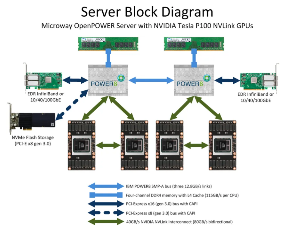
GPU Service Architecture
In distributed systems, the requirements for large model training on computing power infrastructure have expanded from a single card to the cluster level, which places higher demands on the compatibility, transmission efficiency, and latency of large-scale card-to-card interconnect.
Since then, GPU interconnect technology has begun to play an important role.
GPU Interconnect Technology: A Hundred Schools of Thought
02
As everyone knows, the bus is an essential pipeline for data communication, the pipeline through which different hardware on the server motherboard communicates with each other, playing a decisive role in data transmission speed.
The most popular bus protocol currently is the PCIe (PCI-Express) protocol proposed by Intel in 2001. PCIe is mainly used to connect the CPU with other high-speed devices such as GPUs, SSDs, network cards, graphics cards, etc. The PCIe 1.0 version was released in 2003, and subsequent versions are typically updated every three years. It has now been updated to version 6.0, with a transmission rate of up to 64GT/s and a 16-lane bandwidth of 256GB/s, continuously improving performance and scalability.
The development of AIGC has greatly stimulated the increase in computing power demand, and the combination of multiple GPU cards has become a trend. The bandwidth of GPU interconnect usually needs to be above hundreds of GB/S, and the data transmission rate of PCIe becomes a bottleneck. Additionally, the serial-to-parallel conversion of PCIe link interfaces can generate significant latency, affecting the efficiency and performance of GPU parallel computing.
At the same time, due to the PCIe bus tree topology and end-to-end transmission method, which limit the number and speed of connections, signals sent by the GPU need to be transmitted to the PCIe Switch for expansion. The PCIe Switch involves data processing, which can cause additional network latency. Furthermore, the separation of the PCIe bus from memory addresses can exacerbate network latency during each memory access.
Therefore, the transmission rate and network latency of PCIe cannot meet the demand, limiting system performance.
Driven by market demand and technology, GPU interconnect technologies such as GPUDirect/NVLink/Infinity Fabric/high-speed Ethernet/InfiniBand have emerged in competition, marking the beginning of the "Hundred Schools of Thought" era.
GPUDirect
In this process, NVIDIA was the first to introduce GPUDirect, a technology that can enhance GPU communication performance. GPUDirect allows GPUs to directly access the video memory of target GPUs through PCIe, enabling direct communication and data transfer between GPUs and other devices. This significantly reduces the latency of data exchange.
Traditionally, when data needs to be transmitted between a GPU and another device, the data must pass through the CPU, resulting in potential bottlenecks and increased latency. With GPUDirect, network adapters and storage drives can directly read and write GPU memory, reducing unnecessary memory consumption, reducing CPU overhead, and lowering latency, thereby significantly improving performance. GPUDirect technologies include GPUDirect Storage, GPUDirect RDMA, GPUDirect P2P, and GPUDirect Video.
However, due to some limitations of the PCIe bus protocol and topology, higher bandwidth cannot be achieved. After that, NVIDIA proposed the NVLink bus protocol.
NVLink Becomes Mainstream
In the past, we have seen many introductions to NVIDIA's GPU and CUDA moat. Indeed, after years of investment, they have established an insurmountable advantage. However, in addition to this, NVIDIA has many invisible moats, and NVLink is one of them, a technology that provides high-speed connectivity for GPU-to-GPU interconnect.
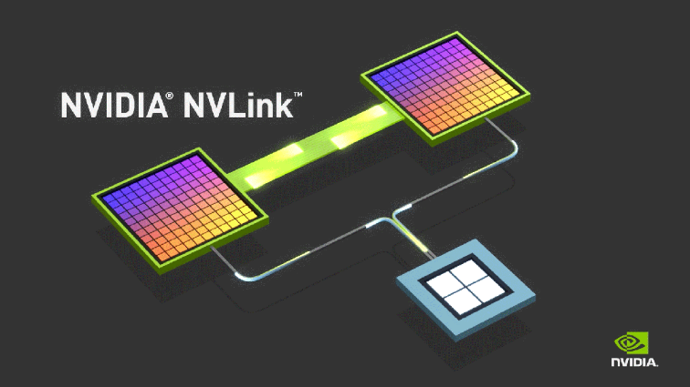
NVLink is a high-speed GPU interconnect protocol proposed by NVIDIA, used to connect multiple GPUs or connect GPUs with other devices (such as CPUs, memory, etc.). It allows point-to-point communication between GPUs, providing higher performance and efficiency for multi-GPU systems compared to traditional PCIe buses.
Compared to the traditional PCIe bus protocol, NVLink makes significant changes in three main areas:
1) Support for mesh topology to solve the limited channel issue;
2) Unified memory, allowing GPUs to share a common memory pool, reducing the need for data replication between GPUs, thereby improving efficiency;
3) Direct memory access, without the need for CPU involvement, GPUs can directly read each other's memory, reducing network latency.
NVIDIA officially stated that NVLink is the world's first high-speed GPU interconnect technology. As a bus and its communication protocol, NVLink uses a point-to-point structure and serial transmission to connect GPUs with CPUs supporting NVLink technology. It maximizes the efficiency of communication between CPUs and GPUs when the memory wall cannot be broken through and can also be used for high-bandwidth interconnect between multiple NVIDIA GPUs. Connecting two NVIDIA GPUs using NVLink allows flexible adjustment of memory and performance to meet the highest workload demands of professional visual computing.
Since 2014, NVIDIA has introduced NVLink interconnect technology in its GPUs.
At that time, NVIDIA, which was struggling with insufficient bandwidth, teamed up with IBM, which had higher bandwidth POWER CPUs at the time, to jointly develop the first generation of NVLink.
Looking back at the development of NVLink technology:
In 2014, NVLink 1.0 was released and implemented between P100 GPU chips. There are four NVLinks between two GPUs, each link consisting of eight lanes, with a speed of 20Gb/s per lane. The overall bidirectional bandwidth of the system is 160GB/s, five times that of PCIe 3 x16, which significantly improves the speed of data movement between CPU memory and GPU video memory, enabling GPU-accelerated applications to run significantly faster.
With the launch of computing cards such as P100 and V100, NVLink ushered in its rapid development.
In 2017, NVIDIA introduced the second-generation NVLink, connecting two V100 GPU chips through six NVLink 2.0 connections. Each link is also composed of eight lanes, with the speed of each lane increased to 25Gb/s, achieving a bidirectional system bandwidth of 300GB/s, almost twice that of NVLink 1.0.
At the same time, to achieve full interconnectivity between eight GPUs and solve the issue of uneven communication between GPUs, NVIDIA also introduced NVSwitch technology.
NVSwitch is a technology released by NVIDIA in 2018, designed to solve the problem of full connectivity between multiple GPUs in a single server. NVSwitch allows up to 16 GPUs in a single server node to achieve full interconnectivity, meaning that each GPU can communicate directly with other GPUs without going through the CPU or other intermediaries.
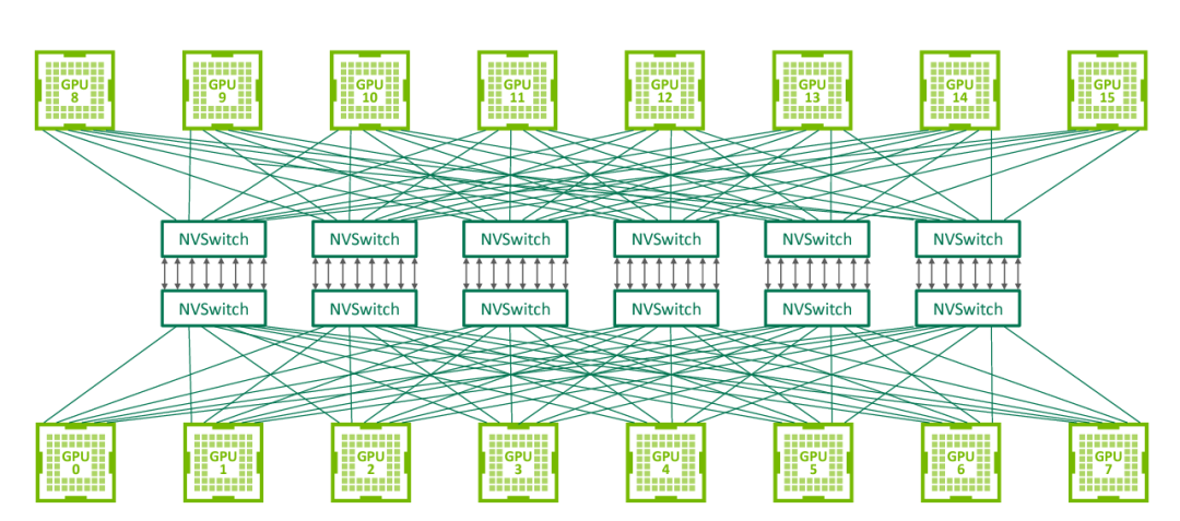
NVSwitch Full Connectivity Topology (Source: nextplatform)
NVSwitch 1.0 has 18 ports, with a bandwidth of 50GB/s per port, for a total bandwidth of 900GB/s. Each NVSwitch reserves two ports for connecting to the CPU. By using six NVSwitches, a fully connected network can be established between eight GPU V100 chips.
In 2020, NVLink 3.0 technology was introduced. It connects two GPU A100 chips through 12 NVLink connections, with each link consisting of four lanes. Each lane operates at a speed of 50Gb/s, resulting in a bidirectional system bandwidth of 600GB/s, twice that of NVLink 2.0. As the number of NVLinks increases, the number of ports on NVSwitch also increases to 36, with each port operating at a speed of 50GB/s.
In 2022, NVLink technology was upgraded to the fourth generation, allowing two GPU H100 chips to interconnect through 18 NVLink links. Each link consists of 2 lanes, with each lane supporting a speed of 100Gb/s (PAM4), increasing the bidirectional total bandwidth to 900GB/s. NVSwitch was also upgraded to the third generation, with each NVSwitch supporting 64 ports, each operating at a speed of 50GB/s.
It is worth mentioning that when the fourth-generation NVLink was released, NVIDIA officially called it NVLink-C2C. At this point, NVLink has been upgraded to a board-level interconnect technology, enabling the connection of two processors into a single superchip within a single package.
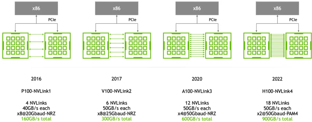
Evolution of NVLink from the first generation to the fourth generation (Source: nextplatform)
In 2024, with the release of NVIDIA's new Blackwell architecture, NVLink 5.0 also came along.
NVLink 5.0 moves data between processors at a speed of 100GB/s. Each GPU has 18 NVLink connections, and the Blackwell GPU provides a total bandwidth of 1.8TB per second to other GPUs or Hopper CPUs, which is twice the bandwidth of NVLink 4.0 and 14 times the bandwidth of the industry-standard PCIe Gen5 bus. NVSwitch has also been upgraded to the fourth generation, with each NVSwitch supporting 144 NVLink ports and a non-blocking switching capacity of 14.4TB/s.
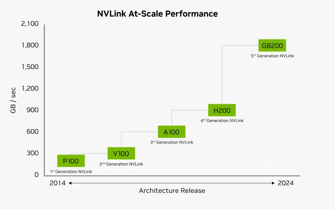
Image Source: NVIDIA
As can be seen from the figure above, with each update of NVLink, the interconnect bandwidth of each GPU has been continuously improving. The number of GPUs that can interconnect between NVLinks has also increased from 4 lanes in the first generation to 18 lanes in the fourth/fifth generation. The speed of each NVLink link has also increased from 20Gb/s in the first generation to the current 1800Gb/s.
In addition, despite its extremely high bandwidth, NVLink consumes much less energy per bit of data transmitted compared to PCIe.
The introduction of NVLink and NVSwitch technologies has brought higher communication bandwidth and lower latency to GPU clusters and deep learning systems, thereby improving the overall performance and efficiency of the system.
With the continuous growth in demand for next-generation AI algorithms and other advanced computing, we can expect further enhancements in the functionality of NVLink. Whether it's an increase in bandwidth or new features that promote better cooperation between GPUs, NVLink or its successors will undoubtedly remain at the core of meeting future computing needs.
It is evident that while competitors are still catching up to NVIDIA's GPU performance, NVIDIA is already making efforts in the innovation of the entire data center architecture layer. By providing faster chip interconnect, stronger computing power scheduling capabilities, NVIDIA packages GPUs into comprehensive data factories with unparalleled performance, delivering them to the world.
AMD Doubles Down on Infinity Fabric
AMD has also introduced Infinity Fabric technology, similar to NVIDIA's NVLink.
Infinity Fabric consists of two parts: Data Fabric and Control Fabric. The Data Fabric is used for data transmission within and between processors; the Control Fabric is responsible for managing the processor's power consumption, clock, and security aspects. This technology supports data transmission between chips, chip-to-chip, and node-to-node.
The main features of Infinity Fabric include:
High Efficiency: Infinity Fabric is designed to provide high-efficiency data transmission, supporting high-speed communication between multiple devices;
Modularity: Infinity Fabric supports AMD's Chiplet architecture, allowing different functional chip modules to be combined through high-speed interconnects;
Memory Sharing: Infinity Fabric supports memory sharing between CPUs and GPUs, helping improve heterogeneous computing efficiency;
Scalability: The design of Infinity Fabric allows it to scale as technology progresses and demand grows.
Infinity Fabric is a key feature introduced by AMD in its "Zen Microarchitecture," aimed at improving overall system performance, especially in multi-core processors and data center environments.
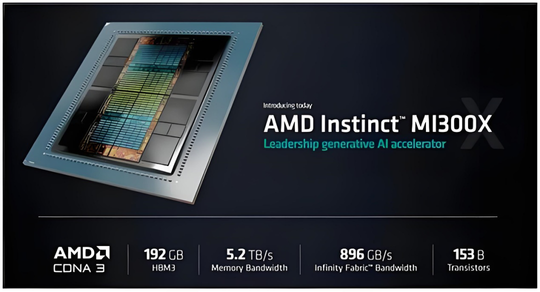
Image Source: AMD
It is reported that AMD's latest AI accelerator, Instact MI300X platform, integrates 8 fully connected MI300X GPU OAM modules into industry standard OCP design through the fourth generation Infinity Fabric link, providing up to 1.5TB HBM3 capacity for low latency AI processing. The fourth generation Infinity Fabric supports up to 32Gbps per channel and generates a bidirectional bandwidth of 128GB/s per link.
Unlike NVLink, which is limited to internal use only, AMD has begun to open up its Infinity Fabric ecosystem to partners and improve its ecological layout.
Chip giants form a group to wage war on Nvidia NVLink
Although GPU interconnection technology may seem diverse, the main technological route is still firmly in the hands of Nvidia, and the industry has been looking forward to some kind of "super" competitor alliance to fill the gap in non Nvidia interconnection technology or clusters.
And this is also an important reason for the launch of UALink, sparking a wave of benchmarking against NVLink.
At the beginning of the article, it is mentioned that eight companies, including AMD, Broadcom, Cisco, Google, HP, Intel, Meta, and Microsoft, have announced the development of a new interconnect technology called UALink (Ultra Accelerator Link) for the network of artificial intelligence data centers. By establishing an open standard for communication between AI accelerators, we aim to challenge Nvidia's dominant position as an AI accelerator company.
According to reports, the first standard version proposed by UALink, UALink 1.0, will connect up to 1024 GPU AI accelerators to form a computing "cluster" to jointly complete large-scale computing tasks.
According to the UALink promotion team, based on "open standards" including AMD's Infinity Fabric, UALink 1.0 will allow direct loading and storage between the memory attached to AI accelerators, and overall improve speed while reducing data transfer latency compared to existing interconnect specifications.
It is reported that UALink will establish a UALink alliance in the third quarter to define high-speed, low latency interconnections for extended communication between accelerators and switches in AI computing cabins, in order to oversee the future development of UALink specifications. UALink 1.0 will be available to companies joining the alliance during the same period, and the updated specification UALink 1.1 with higher bandwidth is planned to be launched in the fourth quarter of 2024. These specifications will support multiple transmissions, including PCI-Express and Ethernet.
The UALink Alliance aims to create an open industry standard that allows multiple companies to add value to the entire ecosystem, thereby avoiding technological monopolies.
The potential advantage of this technology is that it provides everyone in the industry with the opportunity to stay in sync with Nvidia. It is not only suitable for large enterprises, but also opens a door for everyone in the industry to keep up with Nvidia not only in terms of scale, but also in terms of innovation.
Multi machine interconnection:
InfiniBand coexists with Ethernet network
03
In addition, in distributed systems, it can be divided into single card, multi card, and multi machine interconnection according to the different connection levels. In large-scale computing, high bandwidth communication network technologies such as GPU Diect and NVLink are often used in single machine multi card scenarios. In distributed scenarios, connections between multiple machines (i.e. server interconnection) are usually made using RDMA networks.
With the huge demand for computing power in applications such as big data analysis and AI computing, the single machine form mentioned above is gradually unable to meet user needs. Multi machine and multi card computing has become the norm, and communication between multiple machines is an important indicator affecting distributed training.
The communication technologies commonly mentioned in the industry for GPU cards between multiple machines include RDMA, GPU Direct RDMA, and InfiniBand.
RDMA is a technology that bypasses remote hosts and directly accesses data in their memory, solving the problem of remote memory direct access caused by data processing delays in network transmission.
Simply put, RDMA is like a technique that removes intermediaries, allowing data to be quickly obtained. No longer waste time on operating systems, CPUs, and other processes.
At present, RDMA has three different technical implementation methods: Infiniband, RoCE, and iWARP, with the latter two based on Ethernet technology.
For a long time, Ethernet has been the mainstay of computer networks, for example, Intel's Gaudi series AI processors integrate dozens of 100Gb Ethernet connections on the chip; In contrast, Nvidia has monopolized the high-performance InfiniBand interconnect market by acquiring Mellanox.
InfiniBand is an open standard network interconnect technology with high bandwidth, low latency, and high reliability, playing a crucial role in Nvidia's AI factories and supercomputers.
InfiniBand is typically superior to Ethernet in data intensive tasks such as artificial intelligence. According to Dell'Oro's estimate, approximately 90% of AI deployments use InfiniBand instead of Ethernet. These deployments will push Nvidia's network revenue to $10 billion annually.
Intel, betting on Ethernet
Intel's Gaudi AI chips have always used traditional Ethernet interconnection technology.
It is understood that Gaudi 2 uses 24 100Gb Ethernet links per chip; Gaudi 3 doubled the bandwidth of these links by using 24 200Gbps Ethernet RDMA NICs, resulting in a total external Ethernet I/O bandwidth of 8.4TB/s for the chip.
Not long ago, Intel also announced that it is developing an AI NIC ASIC for Ultra Ethernet Consortium (UEC) compatible networks and an AI NIC microchip. These innovative AI high-speed interconnect technologies will be used in its future XPU and Gaudi 3 processors. These innovations aim to revolutionize AI high-speed interconnection technology that can scale vertically and horizontally.
The Ultra Ethernet Alliance (UCE) is a consortium led by Intel AMD、HPE、Arista、Broadcom、 An organization jointly created by Cisco, Meta, and Microsoft to break Nvidia's monopoly. UCE believes that by adjusting the architecture of Ethernet, the performance of the next generation of high-speed Ethernet can be as good as that of InfiniBand networks, with greater cost and openness advantages, thereby attracting more enterprises to join.
Intel has always hoped to win over customers who do not want to invest in proprietary interconnect technologies such as InfiniBand by adopting pure Ethernet switches.
Although InfiniBand performs well in many situations, it also has drawbacks, such as being able to only be used within a specific range (for example, InfiniBand is suitable for users running small to very large workloads (such as GPT3 or digital twins), but Ethernet is usually preferred in more dynamic, ultra large scale and cloud environments), and the cost is not low. Upgrading the entire network to InfiniBand requires a significant investment. In contrast, Ethernet has always been popular in the field of network technology due to its strong compatibility, moderate cost, and ability to handle most workloads, establishing a vast "Ethernet ecosystem".
AMD also stated that it will focus on supporting Ethernet, especially the Ultra Ethernet Alliance. Although Infinity Fabric provides consistent interconnection between GPUs, AMD is promoting Ethernet as its preferred GPU to GPU network.
Overall, in the battlefield of high-performance long-distance transmission, there are only two major camps left: InfiniBand and next-generation high-speed Ethernet, each with its own advantages and disadvantages.
According to Dell'Oro, InfiniBand is expected to maintain its leading position in the field of AI switching in the foreseeable future. However, driven by cloud and ultra large scale data centers, Ethernet will achieve significant growth and is expected to occupy approximately 20% of the market share by 2027.
Future Innovation Trends in Internet Technology
04
It is undeniable that the above-mentioned interconnection technologies are currently the best choices. But it can be foreseen that with the explosive growth of future computing data, the increasing complexity of neural networks, and the accelerated evolution of AI technology, the demand for higher bandwidth continues to grow.
Currently, these interconnected technologies will inevitably face performance bottlenecks.
For example, NVLink from Nvidia, although fast, also has a relatively high power consumption; AMD's Infinity Fabric is suitable for internal chip connections, but the efficiency of interconnection between chips is not ideal.
In this regard, optical interconnection, with its advantages such as high bandwidth and low power consumption, has almost become a recognized development direction for future AI interconnection technology.
On the path of optical connectivity, Google, Broadcom, Marvell, Cisco, and Celestial AI Ayar Labs、Lightmatter、Coherent、 New and old manufacturers such as Xizhi Technology are constantly making efforts and have achieved a series of results.
With the participation of numerous manufacturers, internet technology will experience rapid development in the future. Especially in the field of AI, optical interconnection centered around optoelectronic co packaging and silicon photon relay layer technology is becoming a hot track.
epilogue
05
In the era of big models, computing power is productivity.
Behind a large model lies enormous computational resources, and model size and training data size become key factors determining model capability. Currently, the main players in the market are using tens of thousands of GPUs to build large artificial intelligence clusters to train LLMs.
Under this trend, distributed communication technology is driving the progress of artificial intelligence at an unprecedented speed.
From PCIe to NVLink, Infinity Fabric to InfiniBand, Ethernet, and UALink, these technologies achieve high-speed interconnection between GPUs or AI servers through high bandwidth and low latency data transmission, playing a crucial role in improving the training efficiency and computational performance of deep learning models.
In the rapid development of AI technology, internet technology, as a bridge of the AI era, is also undergoing unprecedented innovation and transformation.


