IBM Develops Co-Packaged Optics Technology to Turbocharge AI Model Training
![]() 12/23 2024
12/23 2024
![]() 715
715
Preface:
The innovative co-packaged optics technology has the potential to supplant electrical interconnects in data centers, dramatically enhancing the speed and energy efficiency of AI and other computational applications.
Author | Fang Wensan
Image Source | Network

IBM's Revolutionary Co-Packaged Optics Technology
Recently, IBM unveiled a groundbreaking optics technology capable of training AI models at lightning speed while significantly reducing energy consumption.
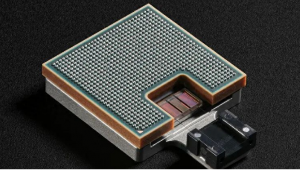
According to IBM's technical paper, this technology represents a new form of co-packaged optics that leverages the speed of light for internal data center connectivity, replacing traditional copper cables.
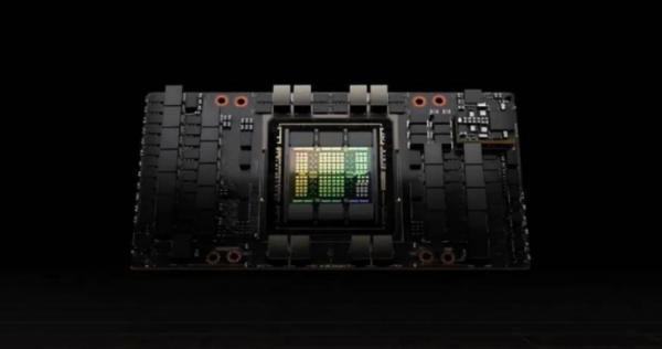
While fiber optics are extensively used in global commerce and communications, most data centers continue to rely on copper cables for short-distance communication. This often results in GPU accelerators remaining idle during training, leading to significant time and energy wastage.
Therefore, IBM's research team demonstrated how to integrate the speed and capacity of light into data centers, substantially increasing communication bandwidth, minimizing GPU idle time, and accelerating AI model processing speeds.

Core Concept of Co-Packaged Optics Technology
Co-packaged optics technology integrates lasers, modulators, photodetectors, and other optical components with electronic components within a single chip. This not only enhances product integration and reliability but also substantially reduces system costs and complexity.
Through fiber optic connections, CPO chips facilitate high-speed, efficient optical transmission and processing, significantly boosting system performance.
CPO is not a novel technology. A year ago, TSMC collaborated with leading companies like Broadcom and NVIDIA to advance the technology, extending the process from 45nm to 7nm, with plans to start receiving large orders in 2024 and achieve mass production by 2025.

80 Times Faster Communication Bandwidth Than Existing Inter-Chip Links
With the rapid advancement of chip technology, modern chips can now accommodate more and denser transistors. IBM's 2-nanometer chip technology, for instance, can embed over 50 billion transistors on a single chip.
Building on this technological foundation, co-packaged optics technology aims to enhance interconnect density between accelerators, enabling chip manufacturers to integrate optical pathways into electronic modules, thereby surpassing the bandwidth limitations of existing electrical pathways.
IBM's new high-bandwidth density optical structure and related innovations, which transmit multiple wavelengths per optical channel, are expected to increase inter-chip communication bandwidth by 80 times compared to electrical connections.

Increasing the Number of Fiber Optic Connections
Compared to the most advanced co-packaged optics technologies, IBM's innovations enable chip manufacturers to multiply the number of fiber optic connections on the edge of silicon photonic chips by six times, termed 'beachfront density.'
Each fiber, approximately three times the width of a human hair, can vary in length from a few centimeters to several hundred meters, transmitting terabits of data per second.
This significantly bolsters data transmission capabilities within data centers, supporting rapid processing of large-scale data.
Ensuring Stability Through Rigorous Testing
The IBM team encapsulated high-density polymer optical waveguides (PWG) on 50-micron spaced optical channels using standard packaging processes and adiabatically coupled them with silicon photonic waveguides.
Remarkably, the co-packaged optics module, utilizing 50-micron spaced polymer optical waveguides, successfully passed all manufacturing-related stress tests for the first time.
These tests included high-humidity environments, extreme temperatures ranging from -40°C to 125°C, and mechanical durability tests, ensuring that the optical interconnects remain intact and data transmission is uninterrupted even under complex conditions like bending, providing a solid guarantee for reliable application in real data center environments.

Simple Principle but Challenging Practical Implementation
The so-called 'silicon photonic chip' replaces transistors in traditional chips with optical components on a silicon platform to transmit electrical and optical signals. Compared to traditional chips, which may experience signal loss and degradation, optical signals exhibit minimal loss, enabling higher bandwidth and faster data processing.
Firstly, there is not yet a large-scale demand for silicon photonic products. Although there is demand in autonomous driving and data centers, no mainstream chip manufacturers have introduced high-performance silicon photonic chips.
Secondly, the cost of silicon photonic products is relatively high. Due to the numerous optical components required, a silicon photonic device employs various materials. In the absence of large-scale demand, silicon photonic products become 'high-priced and low-value.' Additionally, device performance and yield are challenging to guarantee.
Finally, silicon photonic chips still face various challenges. While EDA tools are available for design, they are not specialized. In terms of manufacturing and packaging, major foundries like TSMC and Samsung do not provide silicon photonic process foundry services.
Even TSMC, which has introduced COUPE technology, will focus on more mature packaging solutions in the short term and struggle to allocate capacity for silicon photonic chips.
Conclusion:
Amidst growing demands for AI performance, co-packaged optics technology opens a new communication pathway and could replace external module communications from electronics to optics. This technological breakthrough solidifies IBM's leadership in semiconductor innovation.
Source: PR Newswire: IBM Announces Key Breakthrough in Optics Technology, Ushering in the 'Speed of Light Era' for Generative AI; Mgike.com: IBM Officially Announces New Optics Technology, Can Light Be Used to Train AI?


