Revolutionizing Cooling for AI Chips: Overcoming the Power Consumption Cliff
 05/09 2025
 719
719
The power consumption and heat generation of AI chips profoundly impact the cost, risk, stability, and lifespan of these chips for enterprises. When chips overheat or experience short circuits, the effectiveness and efficiency of AI training and inference can be severely compromised.
A transformative evolution in cooling technology is imperative.
01 AI Chip Power Consumption Crisis
Statistics reveal that global data volume was approximately 10EB in 2015, poised to skyrocket to 175ZB by 2025, potentially reaching an astonishing 2432ZB by 2035. However, the advancement of edge AI encounters two pivotal challenges. Firstly, balancing performance, power consumption, and cost is crucial. How can we optimize results without pushing power consumption and cost to unreasonable heights, especially in low-power, battery-operated devices, while enhancing computational power? Secondly, fostering a robust ecosystem is vital. Similar to the development of CPUs and GPUs, a unified ecosystem encompassing toolchains, languages, compatibility, and ease of development is essential for the widespread adoption and large-scale application of AI technology.
ChatGPT and similar AI bots utilizing large language models (LLMs) to generate human-like conversations are just one of many new AI applications reliant on 'parallel computing'. This term refers to the simultaneous execution of massive computational tasks by a network of chips.
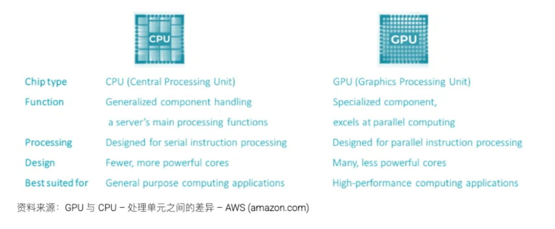
At the heart of AI infrastructure lies the GPU (Graphics Processing Unit), which excels in handling the specialized high-performance parallel computing tasks required for AI. Unlike CPUs (Central Processing Units) used in personal computers, this powerful processing capability also necessitates higher energy input, leading to increased heat output.
High-end GPUs exhibit a power density approximately four times that of CPUs. This poses a significant new challenge for data center planning, as the initially calculated power supply now constitutes only 25% of the power required to operate modern AI data centers. Even cutting-edge hyperscale data centers utilized by Amazon, Microsoft, and Alphabet for cloud computing are still CPU-driven. For instance, Nvidia's current A100 AI chip consumes a constant power of about 400W per chip, while its latest microchip, the H100, consumes nearly twice as much power as the A100, reaching 700W, akin to the power consumption of a microwave oven. If a hyperscale data center with an average of one million servers replaces its current CPU servers with these GPUs, the required power will surge by 4-5 times (1500MW), equivalent to a nuclear power plant!
The increase in power density implies that the heat generated by these chips will also significantly rise. Consequently, the cooling system must be equally robust. Such a scale of power and cooling transformation necessitates a completely novel design for future AI-driven data centers. This will lead to a substantial imbalance in supply and demand at the foundational chip and data center infrastructure levels. Considering the time required for data center construction, industry experts predict that we are in the nascent stages of a decade-long modernization upgrade of data centers aimed at enhancing their intelligence.
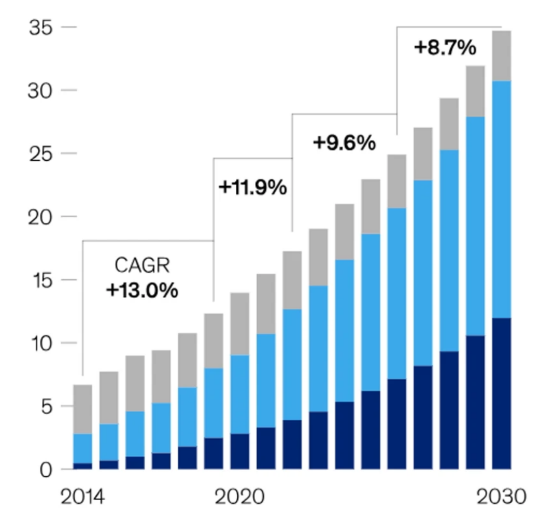
Growth in U.S. Data Center Electricity Consumption (Gigawatts)
02 TSMC's 3DVC Technology
TSMC's 3DVC (3D Vapor Chamber) technology represents an advanced heat dissipation solution tailored for high-performance computing (HPC) and AI chips. It addresses the surge in power consumption and heat generation density stemming from increased integration in advanced process (such as 3nm/2nm) chips.
Traditional vapor chambers feature a two-dimensional planar structure, whereas TSMC's 3DVC employs a three-dimensional design to integrate multiple layers of microfluidic channels directly within the chip package. This leverages phase change heat transfer (liquid evaporation-condensation cycle) to rapidly dissipate heat.
Three-dimensional capillary structure: Internally uses porous metal foam or micro-pillar arrays to bolster the capillary reflow capacity of the working fluid (e.g., water/ammonia).
Near-Junction Cooling: Directly interfaces with the chip's silicon interposer or 3D stack structure (e.g., SoIC) to shorten the heat conduction path.
The heat pipe of the 3D-VC heat sink is a one-dimensional linear heat transfer device. Conventional VC vapor chambers possess an evaporation section and a condensation section, with multiple potential heat dissipation paths depending on the design position, making them two-dimensional heat transfer devices. However, their heat dissipation paths remain confined to the same plane. In contrast to one-dimensional heat conduction heat pipes and two-dimensional heat conduction VC vapor chambers, the heat conduction path of the 3D-VC heat sink is three-dimensional, stereoscopic, and non-planar. The 3D-VC heat sink utilizes a combination of VC and heat pipes to interconnect the internal chambers, enabling working fluid reflow and heat conduction through the capillary structure. The interconnected internal chambers, together with welded fins, form the entire heat dissipation module, facilitating multi-dimensional heat dissipation such as horizontal and vertical.
Comparison of heat pipes, VC, and 3DVC: The multi-dimensional heat dissipation path allows the 3D-VC heat sink to contact more heat sources and offer more heat dissipation paths when dealing with high-power devices. In traditional heat dissipation modules, heat pipes and VC vapor chambers are designed separately. As thermal resistance increases with greater heat conduction distance, the heat dissipation effect is suboptimal. The 3D-VC heat sink extends the heat pipe into the body of the VC vapor chamber. After connecting the vacuum chamber of the VC vapor chamber to the heat pipe, the internal working fluid becomes interconnected. The 3D-VC heat sink is in direct contact with the heat source, and the vertical heat pipe design also accelerates heat transfer speed.
3DVC can be embedded in TSMC's CoWoS 2.5D/3D packaging to provide integrated cooling for CPUs, GPUs, and HBMs. TSMC demonstrated a 3DVC prototype at the IEEE International Electron Devices Meeting (IEDM), which can reduce the junction temperature of 3nm chips by over 15°C. It plans to apply this technology concurrently with the CoWoS-L packaging technology to AMD and NVIDIA's next-generation products.
03 Differences in Cooling Solutions
Liquid cooling stands as the sole viable solution for high-power applications.
The efficiency of heat transfer through the flow of a given volume of liquid far surpasses that of air – water is approximately 3,600 times more efficient. This makes liquid cooling through chip heat sinks an efficient method. When the heat dissipation per square centimeter of chip area exceeds approximately 50 watts, liquid cooling becomes necessary. Considering that the area of GB200 is roughly 9 square centimeters, any heat dissipation exceeding 450 watts necessitates pumped liquid cooling. In 'direct chip' cooling, the liquid flows through cold plate channels connected to the chip heat sink via a thermal interface. When the liquid does not evaporate during this process, it is termed 'single-phase' operation, where the medium (typically water) is pumped through a fan-cooled heat exchanger. Flex's subsidiary JetCool offers direct chip liquid cooling modules that employ a small array of fluid jets precisely targeting hot spots on the processor, thereby enhancing high-power electronic cooling performance at the chip or device level.
Heat can be transferred to a second liquid loop, which can supply hot water for buildings and potentially local consumers. Two-phase operation offers superior heat transfer by allowing the liquid (usually a fluorocarbon) to evaporate when absorbing heat and then recondense at the heat exchanger. This method can significantly boost performance. However, system fans are still required to cool other components, although some components (such as DC/DC converters) can be integrated into the liquid cooling loop using their own substrates. This aligns with the concept of 'vertical power delivery', where DC/DC converters are situated directly beneath the processor to minimize voltage drop. The practical limitation of the direct chip method lies in the thermal resistance at the interface between the chip and the cooling plate. Precise surface flatness and high-performance solder paste are necessary, but temperature differences remain an issue at multi-kilowatt power levels.
To overcome this limitation, immersion cooling technology can be considered. The entire server is submerged in an open dielectric fluid tank, and the dielectric fluid is pumped through a reservoir around a loop to the heat exchanger. Similarly, for optimal performance, two-phase operation can be employed.
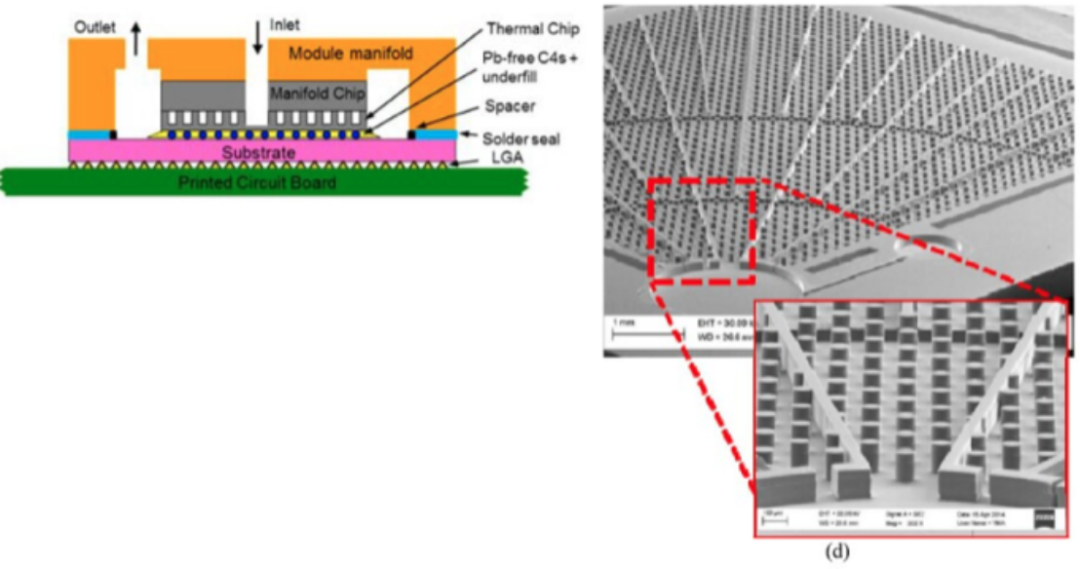
In addition to immersion cooling technology, IBM utilizes embedded microchannel phase change cooling technology. IBM pumps the dielectric fluid directly into microscopic gaps of about 100μm in any level of chip stacking, extracting heat from the chip through the boiling of the dielectric fluid from the liquid phase to the gas phase. They tested a modified IBM Power 7+ chip with this technology, resulting in a 25°C reduction in junction temperature.
To achieve embedded cooling, IBM removed the processor's packaging lid to expose the die, performed deep reactive ion etching (DRIE) on the die, constructed 120μm deep cooling channel structures on its back, and bonded a glass plate to the etched chip to form the top wall of the microchannels. Adhesive was used to bond the coolant inlet and outlet brass manifolds to the glass manifold chip and organic substrate. The coolant enters the module through 24 inlets, distributing flow through the corresponding 24 radially expanding channels.
NVIDIA: Hardware-Level Cooling Integration (NVLinkC2C Technology)
The release of Blackwell heralds a new era in AI hardware, with its formidable performance providing unprecedented computational support for AI companies, enabling the training of more complex and accurate models. AI computing power based on Blackwell will be offered to users in the form of a comprehensive server called DGX GB200, which integrates 36 NVIDIA Grace CPUs and 72 Blackwell GPUs. These superchips are interconnected into a supercomputer through the fifth-generation NVLink to enhance overall computing performance. To better support the application of GB200 superchips, NVIDIA has introduced a new computing cluster, DGX GB200 SuperPod. This supercomputing cluster adopts a novel and efficient liquid-cooled rack-scale architecture, delivering astonishing computing power and memory capacity at FP4 precision. Through DGX GB200 SuperPod, NVIDIA will provide robust AI computing capabilities to various industries, driving the advancement of the AI industrial revolution and once again showcasing its leadership and innovation in the AI field.
Specifically, NVLINK is a high-speed interconnect technology specifically designed to connect NVIDIA GPUs. It enables GPUs to communicate in a point-to-point manner, bypassing the traditional PCIe bus, achieving higher bandwidth and lower latency. NVLINK can be used to link two or more GPUs for high-speed data transmission and sharing, offering higher performance and efficiency for multi-GPU systems.
For instance, the GB200 NVL72 comprises 18 1U servers, delivering 720 petaflops of FP8 performance and 1440 petaflops of FP4 computing performance, capable of handling up to 27 trillion AI LLM parameter models. Each server contains two GB200 Grace Blackwell Superchips, and these computing nodes boast 1.7TB of HBM3E memory and 32TB/s of memory bandwidth. To tackle the issue of excessive power consumption, NVIDIA has opted to adopt liquid-cooled MGX packaging and a liquid-cooled rack-level solution.
-
![]()
Market Share Dilemma: DJI vs. Insta360—Is It '40-40' or '60-30'?
-
![]()
Market Share Dilemma: DJI vs. Insta360 – A '40-40 Split' or '60-30 Split'?
-
![]()
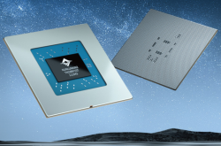
It's Kunlunxin's Turn to Play
-
![]()
Is the New Performance Peak Just the Starting Point? What Will Be Crystal-Optech's Next Destination?
-
![]()
Goertek Pours 69 Million Yuan into Elite Precision: Ramping Up Optical Precision Manufacturing and R&D Capabilities
-
![]()
Avatr Attempts HKEX Listing Again, With 20,000 Vehicles Sold in First Five Months
-
![]()
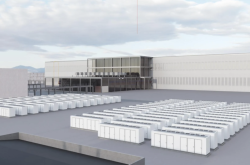
NVIDIA Announces 10-Fold Production Capacity Increase in 2 Years, Disrupting the Energy Storage Industry
-
![]()
AI Enters the Second Half: Models Are No Longer Scarce, What’s Truly Scarce Are Computing Power, Scenarios, and Trust