【Beginner's Guide】What Exactly is PCIe?
![]() 07/15 2024
07/15 2024
![]() 682
682
Hello everyone, I'm Lao Mao.
At the recent 2024 Developer Conference, the Peripheral Component Interconnect Special Interest Group (PCI-SIG) announced the latest progress on PCIe 6.0 and PCIe 7.0.
The deep conformance testing for PCIe 6.0 will commence in 2025, while the final specification for PCIe 7.0 is still scheduled for release in 2025, but the corresponding Live Compliance program has been postponed to 2028. Judging from the reactions at the recent PCI-SIG Developer Conference, it seems that patience is wearing thin among attendees.
These products will initially be used in data centers, followed by industrial, automotive, aerospace, and military applications, and eventually consumer electronics. Delays in any of these stages could potentially push back the entire roadmap.
As a high-speed serial computer expansion bus standard, PCIe has long been ubiquitous in every PC, benefiting both ordinary users and professionals, as well as large and small enterprises alike.
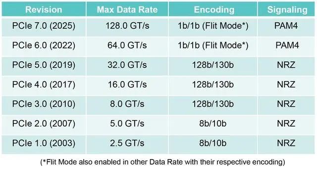
However, this long-standing standard is not static. Over the past two decades, it has undergone six iterations, with the transmission rate per lane increasing from 2.5 GT/s to 128 GT/s, marking a monumental transformation. The latest PCIe 7.0 solution boasts a bidirectional bandwidth of up to 512GB/s for x16 lanes, doubling the previous capacity.
▉ What is PCIe?
PCIe stands for PCI-Express, a high-speed serial computer expansion bus standard.
The word "Bus" in English can refer to a vehicle or, in the context of computers, a bus. These two meanings actually share some similarities. Using a real-life example, a bus is an essential mode of transportation connecting two cities, while a bus in computing serves as a vital connection between different components.
If we want to travel from Tianjin to Beijing, we can take a coach. Similarly, computers rely on the PCIe bus for communication. In simple terms, the bus serves as a highway for communication between multiple hardware components.

Analogous to roads, PCIe also has different specifications. Just like highways have different speed limits, PCIe 1.0, PCIe 2.0, PCIe 3.0, and PCIe 4.0 represent different standards with varying capabilities.
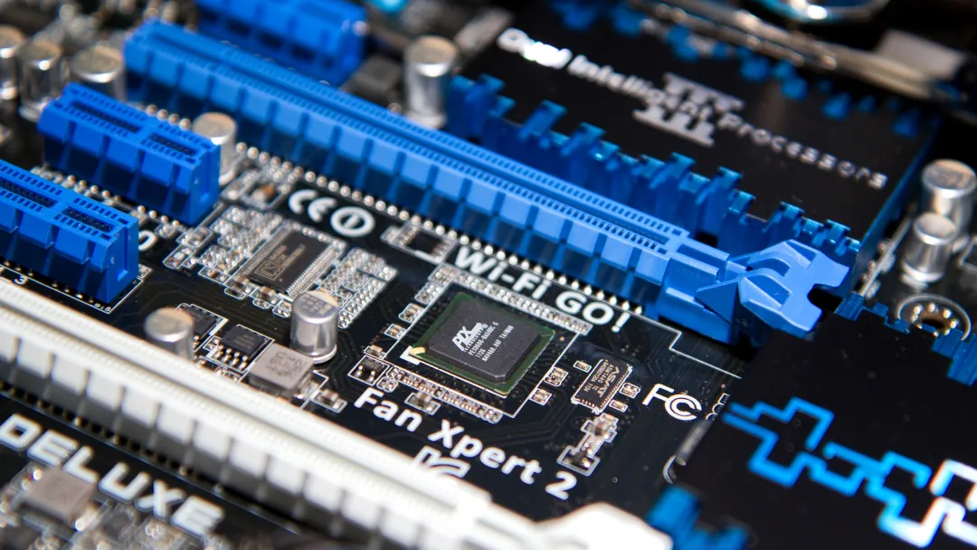
Even on the same highway, different lanes may have different speed limits, similar to how PCIe 1.0 slots with different expansion capabilities (e.g., PCIE x16/x8/x4/x1) support varying maximum transmission speeds.
The PCIe bus is a crucial component of the computer device tree, with almost all peripheral hardware expansions relying on it. Today, let's delve into the history of PCIe.
▉ Exploring the Ancestors of PCIe
Years ago, different devices on a computer motherboard used distinct bus interfaces. Hard drives had their corresponding bus interfaces, and network cards had theirs.
This had the advantage of optimizing performance for each device through dedicated interfaces. However, as the number of expansion devices increased, expanding corresponding bus interfaces on the motherboard became impractical, limiting motherboard expansion and complicating hardware standardization.
To address this bottleneck, IBM and Intel collaborated to introduce the first-generation ISA slot on the IBM PC XT in 1981. As a pioneering work in modern PCs, the 8-bit ISA provided a bandwidth of 4.77MB/s.
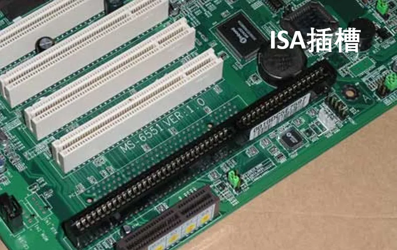
Thanks to its good compatibility, the ISA bus gained popularity among manufacturers and became the most widely used system bus in the 1980s. However, due to its parallel bus design and immature anti-interference technology, the ISA bus could only achieve a bandwidth of 8MB/s, insufficient for the emerging needs of large data transfers like images in the 1990s.
Apart from its slow speed, the ISA bus interface devices could not be autoconfigured or hotplugged. Moreover, IBM's introduction of the MCA bus on the PS/2 product line forced other PC-compatible manufacturers to develop EISA, ultimately leading to the obsolescence of the ISA bus.
In 1992, Intel proposed the PCI (Peripheral Component Interconnect) bus protocol and, leveraging its influence in the PC industry, formed the PCI-SIG (PCI Special Interest Group) enterprise alliance. Since then, this organization has been responsible for standardizing and promoting the PCI bus.
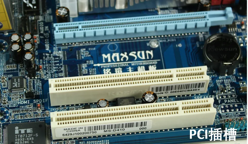
Intel's foresight in establishing its "circle of friends" in the 1990s deserves praise. Unlike the closed IBM, Intel's collaborative mindset facilitated the widespread adoption of the PCI standard. This unified standard also encouraged innovation among peripheral device manufacturers, enriching the PC ecosystem with various PCI devices.
Compared to the ISA bus, the PCI bus boasted a significantly upgraded bandwidth of 132MB/s and supported autoconfiguration and hotplugging.
However, the PCI bus was not perfect. Like the ISA bus, it used a parallel bus design, limiting its transmission speed. Moreover, its bandwidth-sharing mechanism could lead to bandwidth contention under high loads, and it did not support hotplugging.
To address these limitations, technology underwent another upgrade in 2004, when Intel led the development of PCI Express (PCIe), the topic of this article. Today, PCIe has evolved into the fifth generation (Gen 5, 5.0) and become an indispensable component in computers.
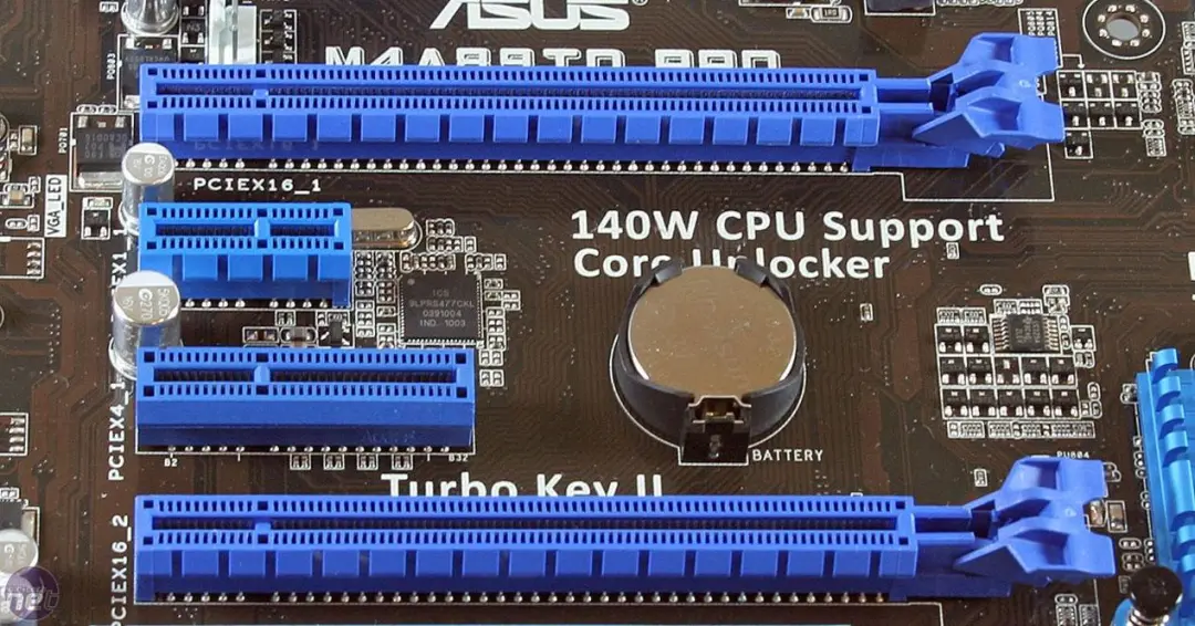
PCIe now supports a wide range of devices, including graphics cards, solid-state drives (in PCIe form factor), wireless network cards, wired network cards, sound cards, video capture cards, PCIe-to-M.2 adapters, PCIe-to-USB adapters, and PCIe-to-Type-C adapters.
▉PCIe Transmission Speed and Lane Width
PCIe buses exist in two forms: interfaces and lanes. When PCIe exists as an interface, it appears as a long slot on the motherboard. Some may wonder about the purpose of these long slots and why they vary in length.
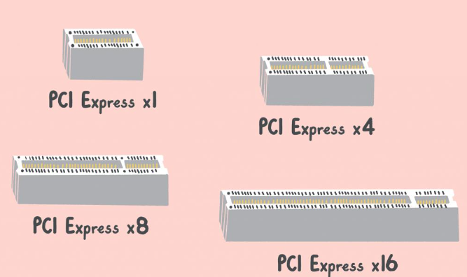
These long slots are actually different PCIe interfaces, with four common sizes: X1, X4, X8, and X16. Generally, the maximum bandwidth of these slots differs, with X16 offering double the speed of X8, which in turn is double that of X4. However, this comparison is based on the same PCIe generation.
So, how is PCIe throughput calculated? The formula is: Throughput = Transmission Rate * Encoding Scheme * Physical Lane Count. For example, in PCIe 4.0 x4, with 4 physical lanes and a transmission rate of 16GT/s using 128b/130b encoding, the throughput per lane is 1.969GB/s, resulting in a total throughput of 7.877GB/s for PCIe 4.0 x4 and 64GB/s for PCIe 4.0 x16.
Apart from throughput differences, what are the specific applications of different PCIe sizes? Let's take a closer look at X1, X4, X8, and X16.
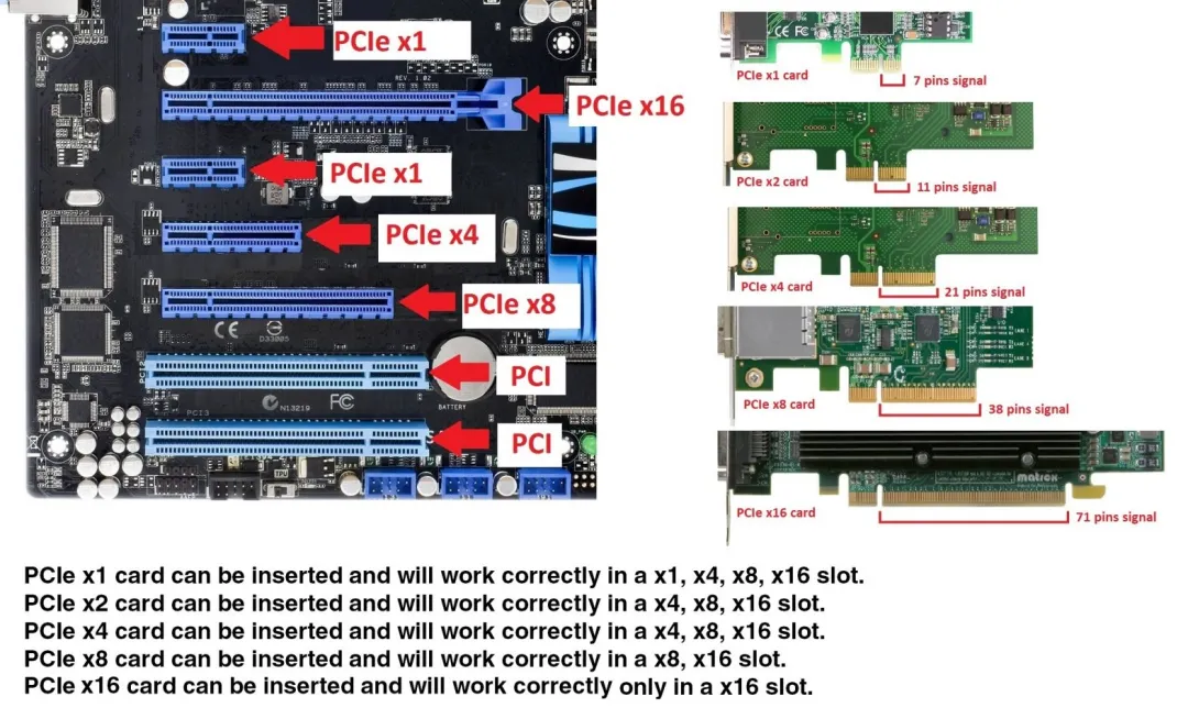
PCIe x16 slot: As shown in the image, the PCIe x16 slot is 89mm long with 164 pins. It has a latch on the outer side, dividing the 16x into two groups. The shorter section with 22 pins is for power supply, a design common to all slot sizes. The longer section with 142 pins is for data transmission, offering high bandwidth through 16 lanes.
Currently, the PCIe x16 slot is primarily used for GPU graphics cards and RAID controller cards. It offers excellent compatibility, supporting devices of x1/x4/x8 levels while delivering superior transmission performance. It can be considered a versatile slot.
Since the PCIe x16 slot is often used for graphics cards, it is physically close to the CPU, facilitating low-latency data exchange between the GPU and processor, thereby maximizing system performance.
PCIe x8 slot: 56mm long with 98 pins, the PCIe x8 slot has 76 data pins compared to the PCIe x16 slot, with the same 22 power pins. For compatibility, PCIe x8 slots are often made in the form of PCIe x16 slots but with only half the data pins active, resulting in half the bandwidth of a true PCIe x16 slot. Observe the motherboard layout to see that the rear half of an x8 slot may lack connections or soldered pins.
Except for flagship or server motherboards, which may offer multiple genuine PCIe x16 slots, most motherboards only provide one genuine PCIe x16 slot closest to the CPU. The second and third PCIe x16 slots are often PCIe x8 or even x4.
PCIe x4 slot: 39mm long, the PCIe x4 slot is implemented by reducing data pins based on the PCIe x16 slot design. It is primarily used for PCIe SSDs or M.2 SSDs installed via PCIe adapters.
PCIe x4 slots are typically expanded by the motherboard chipset, but with the increase in PCIe lanes within CPUs, some high-end motherboards now offer PCIe x4 slots directly connected to the CPU for PCIe SSDs.
Like PCIe x8 slots, PCIe x4 slots are often made in the form of PCIe x16 slots for compatibility or expanded as M.2 interfaces for M.2 SSDs, M.2 wireless network cards, or other M.2 devices, leaving PCIe x1 slots for other expansion cards.
PCIe x1 slot: At just 25mm long, the PCIe x1 slot has significantly fewer data pins (14) compared to the PCIe x16 slot. Its bandwidth is usually provided by the motherboard chipset and is used for independent network cards, sound cards, USB 3.0/3.1 expansion cards, etc. It can even host graphics cards through adapters for mining or multi-monitor setups.
Another important role of PCIe x1 slots is to replace legacy PCI devices.
▉ What Does the Future Hold for PCIe?
Since its inception in 2001, PCIe has established a formidable "moat" in terms of protocol integrity. Redefining an interface protocol to outperform PCIe in the short term lacks both corporate motivation and feasible technological innovations.
Generally, it takes 1-2 years for a specification to reach commercialization, similar to Moore's Law, which predicts product upgrades every 1-2 years.
However, relying on its monopoly, Intel has taken a cautious approach to PCIe upgrades. After PCIe 1.0's release in 2004, PCIe 5.0 began appearing on motherboards only with the launch of new-generation servers in 2023.
PCIe 5.0 marks a significant milestone in PCIe's development, as unexpected demand surges in big data AI, visual rendering, genetic analysis, and EDR simulations have outpaced PCIe's data transmission capabilities, particularly for GPUs.
To address PCIe's data transmission limitations, several alternative transmission and memory-semantic protocols emerged, including IBM's OpenCAPI, Xilinx's CCIX, NVIDIA's NVLink, and HPE's Gen-Z, all aiming to solve PCIe 4.0's speed issues.
Faced with competitors "revolutionizing" PCIe, Intel introduced the CXL (Compute Express Link) protocol in March 2019, encapsulating CXL protocols within PCIe link-layer packets and diverting CXL-specific transactions to dedicated CXL processing logic at the CPU-side PCIe controller.
Intel hopes to enable high-speed, efficient interconnects between CPUs, GPUs, FPGAs, or other accelerators, meeting the demands of high-performance heterogeneous computing. Notably, the CXL standard is compatible with PCIe 5.0, allowing CXL protocols to run on PCIe 5.0, further consolidating PCIe's influence in computing.
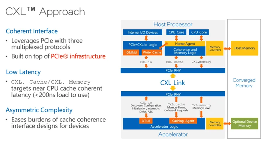
Intel's strategy is to harness the emerging demand trends for GPUs and DPUs as a counterbalance to NVIDIA. Now that NVIDIA has joined the CXL Alliance, Intel has effectively built a "highway" to memory, controlling how GPUs traverse it.

This approach also allows Intel to further balance GPU development, determining how many GPUs a CPU can support.
It's worth noting that the fourth-generation Intel Xeon Scalable processors support up to 4 CXL devices per processor, including CXL Type 1 and CXL Type 2, enhancing server capabilities for memory-intensive and IO-intensive scenarios.
▉Conclusion
PCIe 7.0 is the next-generation computer interconnect technology, aiming to double the data transmission speed per pin to 128 GT/s compared to PCIe 6.0's 64 GT/s and PCIe 5.0's 32 GT/s. This will enable a 16-lane (x16) connection to support 256 GB/s bandwidth in each direction (excluding encoding overhead). Such speeds will be highly beneficial for future data centers, AI, and high-performance computing applications requiring faster data transmission rates.
To achieve impressive data transmission rates, PCIe 7.0 doubles the bus frequency of the physical layer compared to PCIe 5.0 and 6.0. Additionally, it retains pulse-amplitude modulation with four-level signaling (PAM4), 1b/1b FLIT mode encoding, and forward error correction (FEC) technology used in PCIe 6.0. Moreover, the PCI-SIG highlights that the PCIe 7.0 specification focuses on enhanced channel parameters and coverage, as well as improved power efficiency.
Notably, last summer, PCI-SIG announced its exploration of PCIe optical connectivity. To this end, the PCI-SIG Optical Working Group was formed in August 2023 to design appropriate form factors for connectors and transceivers. Optical connectivity technology, transmitting data via light waves, has the potential to expand PCI Express's application domains, such as cloud computing, high-performance computing, and quantum computing. Compared to copper wire transmission, this could offer higher throughput, lower latency, and reduced energy requirements.
For these scenarios, PCIe 7.0 interfaces could potentially reach data transmission rates of 512 GT/s, significantly impacting heterogeneous computing architectures.


