Soaring 14-Fold Profits, Yet This Giant Faces Internal and External Challenges?
 07/18 2024
 734
734
Recently, Samsung Electronics, the world's largest memory chip manufacturer, disclosed its second-quarter earnings report.
Samsung Electronics demonstrated astonishing financial performance in its Q2 2024 earnings report, with operating profit surging 1452% year-on-year to reach 10.4 trillion Korean won (approximately RMB 55.1 billion). This figure not only significantly exceeded market analysts' general expectations but also marked a notable turnaround in Samsung's profit situation since the second half of 2022.
01
AI Demand Soars, Boosting Samsung and SK Hynix to Turn Losses into Gains and Soar in Performance
Samsung's Q2 performance far exceeded market expectations, with profits surging 14-fold.
However, in the second half of 2022, Samsung Electronics faced a marked decline in its Device Solutions Division and overall profits, with operating profit once falling below 1 trillion Korean won. Nevertheless, starting from the second half of 2023, as the market environment improved, Samsung's profits began to rebound, with operating profits for both the third and fourth quarters returning to over 2 trillion Korean won. In 2024, the first-quarter operating profit reached 6.61 trillion Korean won, representing a tenfold increase from the same period last year's 0.64 trillion Korean won.
As AI demand surges, leading to intensified memory competition, Samsung plans to raise DRAM and NAND prices by 15% to 20% in the third quarter, and it is expected that Samsung's second-half performance will also improve.
Meanwhile, another Korean memory chip giant, SK Hynix, also achieved significant earnings growth in the second quarter. SK Hynix will announce its Q2 financial results on July 26. Market projections suggest that its operating profit will reach 5 trillion Korean won (approximately RMB 26.35 billion), setting a six-year high record. This indicates that the entire memory chip industry is benefiting from the growth in AI-related demand, particularly in the area of high-bandwidth memory (HBM), with a projected compound annual growth rate (CAGR) of 70% over the coming years.
Statistics show that at least 19 analysts have raised their forecasts for the company over the past month, citing the huge potential of AI demand and the possibility of positive surprises from the financial report released this month.
Goldman Sachs Group raised its target price for SK Hynix to 290,000 Korean won. Citigroup also increased its target price for SK Hynix to 350,000 Korean won.
Roh Jongwon, Chief Investment Officer at Infinity Global Asset Management, said that SK Hynix's share price valuation does not fully reflect the potential of high-bandwidth memory (HBM), which generates nearly double the profits of traditional DRAM chips, but the market currently values both products equally.
In the second quarter of last year, SK Hynix's operating loss reached 2.88 trillion Korean won, up 15% quarter-on-quarter; net loss reached 2.99 trillion Korean won, down 16% quarter-on-quarter; quarterly operating loss rate was 39%, and net loss rate was 41%. However, with the emergence of AI, this predicament has taken a turn for the better.
In the first quarter of this year, SK Hynix's consolidated revenue reached 12.4296 trillion Korean won, operating profit was 2.886 trillion Korean won, and net profit was 1.917 trillion Korean won. First-quarter revenue hit a record high for the same period, while operating profit was the second-highest for the same period. Leveraging its technological leadership in AI-oriented memory such as HBM, SK Hynix increased sales of AI server-oriented products while continuing to implement profit-focused business activities, achieving an operating profit growth of 734% quarter-on-quarter.
This explosive growth in performance is primarily attributed to the surge in demand for artificial intelligence (AI), which has directly driven up memory chip prices. As the world's largest memory chip suppliers, Samsung Electronics and SK Hynix occupy advantageous positions in the AI wave, benefiting from the robust demand for high-performance storage solutions (primarily HBM) from data centers, cloud computing, and various smart devices.
AI servers need to process large amounts of parallel data, requiring high computing power and large bandwidth. High computing power means AI servers process data faster, while large bandwidth allows servers to access more data simultaneously. HBM meets the AI servers' need for efficient data processing by providing high bandwidth and low latency, making AI model training and inference processes faster and more efficient. This is the primary driver behind the annual growth in HBM market demand.
In this context, HBM has become the "standard configuration" for mainstream AI training chips in the current market. A research report from Zhongtai Securities in March this year noted that current mainstream AI training chips are equipped with multiple HBMs. Taking NVIDIA's AI training chip H100 as an example, one NVIDIA H100 chip uses TSMC's packaging technology to encapsulate seven chips (one GPU + six HBMs) together.
In May, renowned market research firm DIGITIMES released a report stating that the global value of server GPUs (including boards and subsystems containing memory) will reach US$121.9 billion in 2024, with the proportion of high-end server GPU value exceeding 80% at US$102.2 billion.
As a key component of AI training chips, HBM orders have surged along with AI servers.
02
Memory Giants Continue to Increase Production and Expand Layout
During the earnings conference calls of SK Hynix and Micron Technology, executives from both companies stated that their HBM orders have been fully booked, with capacities sold out until 2025. Samsung Electronics also emphasized during its Q1 2024 earnings conference call: "In 2024, our HBM bit supply has actually increased more than three times compared to last year. We have completed relevant supply discussions with customers. In 2025, we will continue to expand supply, increasing at least twice or more than last year."
Faced with overwhelming order demand, memory giants are stepping up their layouts.
During SK Hynix's Q1 2024 earnings conference call, the company's management stated that to actively support the growing demand for AI memory and traditional DRAM, it had decided to invest in the construction of a new DRAM production base, M15X, with the goal of commissioning it by the end of 2025.
Additionally, SK Hynix has decided to build an advanced AI memory packaging production facility in West Lafayette, Indiana, USA, with a total investment of approximately US$3.87 billion. This facility will commence mass production of next-generation AI memory products, including HBM, from 2028.
SK Hynix is expanding its 5th-generation 1b DRAM to address the increased demand for HBM and DDR5 DRAM. SK Hynix has placed orders with multiple equipment companies. Through this investment, SK Hynix's 1b DRAM production capacity is expected to increase from 10,000 wafers per month in the first quarter to 90,000 wafers per month by the end of the year. SK Hynix also plans to increase 1b DRAM production to 140,000 to 150,000 wafers per month by the first half of next year.
On June 30, SK Group, the parent company of SK Hynix, stated that by 2028, SK Hynix will invest 103 trillion Korean won (US$74.6 billion) to strengthen its chip business, focusing on artificial intelligence. SK Group also plans to secure 80 trillion Korean won in funds by 2026 for investments in AI and semiconductors, funding shareholder returns, and streamlining over 175 subsidiaries.
Samsung is not far behind, with plans to introduce 3D packaging services for high-bandwidth memory (HBM) within the year. The company plans to use this packaging method for its sixth-generation HBM chip, HBM4, which is scheduled for release next year.
According to reports, Samsung Electronics has once again reorganized its HBM memory team, adjusting the advanced packaging organizational structure. Samsung previously established an HBM Capacity and Quality Improvement Team dedicated to HBM4 development, operating in parallel with the original HBM team. The newly established "HBM Development Team" will replace the previous two teams, overseeing the development of both HBM3E and HBM4 memory, concentrating human and material resources on catching up with industry leader SK Hynix in the HBM business. Samsung Electronics has also renamed its advanced packaging business team as the "AVP Development Team," splitting the original team's sales and marketing organization into various business units and incorporating HBM packaging developers into the HBM Development Team to enhance its competitiveness.
Samsung Electronics has also decided to reorganize its Device Technology Institute to strengthen technical support capabilities for semiconductor processes and equipment, providing broader technical support for improving semiconductor process efficiency.
Samsung Electronics is also upgrading its plant in Pyeongtaek, South Korea, with an estimated completion date of April 2027.
Additionally, Micron is catching up, with news that its next-generation HBM offers advantages in power consumption over SK Hynix and Samsung Electronics. Micron Technology plans to expand its production line in Hiroshima, Japan, with an estimated investment of JPY 600 billion to JPY 800 billion (approximately US$5.1 billion). This new plant will commence construction in early 2026 and install EUV equipment.
03
HBM4 Becomes a Competitive Hotspot
As major players continue to invest, HBM technology iterations are accelerating. The JEDEC Solid State Technology Association, an industry standards organization, recently stated that the HBM4 standard is nearing finalization, offering higher bandwidth, lower power consumption, increased die/stack performance, and further improved data processing rates. Compared to HBM3, HBM4 doubles the number of stack channels per stack and has a larger physical size.
Vendors are also vying for supremacy around future HBM4 technology.
SK Hynix is advancing TSV and MR-MUF technology development, which play crucial roles in HBM performance. While MR-MUF is widely used, it has drawbacks such as susceptibility to warping, causing wafer end bending and void phenomena (uneven distribution of protective materials in certain areas), which negatively impact MR-MUF reliability. SK hynix stated that compared to the early stages of HBM development, they have successfully reduced warping phenomena and are currently developing technologies to overcome this issue. The next step will focus on reducing voids.
Moreover, SK Hynix is committed to developing next-generation advanced packaging technologies such as chiplets and hybrid bonding to support heterogeneous integration between semiconductor memory and logic chips, while promoting the development of new semiconductor types. Among them, hybrid bonding is seen as another new option for HBM packaging. However, unlike previous plans, SK Hynix intends to continue using the cutting-edge packaging technology MR-MUF in the next-generation HBM 4. The hybrid bonding technology, which emerged as an alternative, is expected to be introduced gradually due to the relaxation of HBM standards.
In April this year, SK Hynix signed a memorandum of understanding with TSMC to jointly produce the next-generation HBM and improve the integration of logic and HBM through advanced packaging technology. The company plans to develop HBM4, the sixth-generation product in the HBM series, through this initiative, with mass production expected to start in 2026. The two companies will first focus on improving the performance of the base chip installed at the bottom of the HBM package and have agreed to collaborate on optimizing the integration of SK Hynix's HBM and TSMC's CoWoS technology to address customers' shared requirements for HBM.
Unlike SK Hynix, Samsung adopts TC-NCF (thermal compression with non-conductive film) for HBM packaging. With advancements, Samsung has gradually reduced the thickness of NCF material, reducing the thickness of the 12-layer fifth-generation HBM3E to 7 micrometers (μm).
Samsung Electronics concentrated efforts company-wide and announced the "Advanced TC-NCF" technology in February. This technology can reduce the thickness of the necessary film in the TC-NCF process, thereby increasing the number of semiconductor layers while maintaining HBM height.
Samsung Electronics applied MOSFET technology to HBM3E and is actively considering applying FinFET technology starting with HBM4. As a result, compared to MOSFET application, HBM4 offers a 200% speed increase, a 70% area reduction, and over 50% performance improvement. This is the first time Samsung Electronics has publicly disclosed HBM4 specifications.
Reports indicate that Samsung Electronics recently formulated an internal plan to replace the 1b DRAM originally planned for installation in HBM4 with 1c DRAM.
Additionally, according to South Korean media etnews, Samsung Electronics and SK Hynix have begun transitioning their high-bandwidth memory (HBM) wafer process technology, with the introduction of new technology to prevent wafer warping as the core focus. This transition is considered targeted at next-generation HBM. It is expected that with the process transition, changes will also occur in the materials and equipment supply chain. It is reported that Samsung Electronics and SK Hynix are currently working with partners to develop a laser method for debonding (detaching) HBM wafers, replacing the existing mechanical method.
When lasers are applied, changes in related materials and equipment supply chains are inevitable. The existing mechanical method is dominated by Tokyo Electron of Japan and SÜSS MicroTec of Germany. The laser method is expected to attract more equipment companies, potentially leading to intense competition.
04
Samsung Still Faces Internal and External Challenges
Although Samsung is benefiting from the industry recovery driven by the AI boom, the tech giant is not completely at ease.
In the crucial HBM chip sector of the AI boom, Samsung faces fierce competition from SK Hynix. It is reported that Samsung Electronics' HBM3e (high-bandwidth memory) chip passed NVIDIA's quality tests, and Samsung will negotiate for large-scale production of HBM and supply to NVIDIA.
In May this year, it was reported that Samsung's latest HBM chip had not passed NVIDIA's tests. Sources claimed that the primary reason Samsung's product failed the test was that TSMC "adopted test standards based on SK Hynix's HBM3E product settings" during testing. Subsequently, Samsung Electronics stated that claims that the chip had not passed testing due to heating and energy consumption issues were "untrue," and that "testing is proceeding smoothly and as planned."
Furthermore, Samsung faces internal management challenges: Just days before announcing its earnings, Samsung union organizers planned a three-day strike among its over 28,000 members, including those in major chip factories, due to wage disputes. Last month, the company saw its first strike in 55 years, involving a small number of employees.
On July 10 local time, the largest labor union of Samsung Electronics, the "National Samsung Electronics Labor Union," announced the launch of an indefinite general strike. The union had originally planned a three-day strike starting from the 8th, followed by a five-day strike starting from the 15th. However, due to the management's lack of willingness to engage in dialogue, the union decided to initiate an indefinite general strike.
This strike may reflect Samsung Electronics' deteriorating operating conditions in recent years. Industry insiders stated that Samsung Electronics failed to respond timely to market demand in the semiconductor industry and AI chip sector, resulting in losses in the company's semiconductor business last year. The union pointed out that the root cause of this crisis lies in management's decision-making errors, not the responsibility of employees.
-
![]()
Total Investment Hits Nearly 3.28 Billion! Goertek Launches Mass Production of 12-Inch Transparent Substrate Wafer for AR Glasses’ Micro-Nano Optical Components
-
![]()
Why Is This Precision Optical Film Leader Worth Reevaluating with a Tens of Millions Procurement?
-
![]()
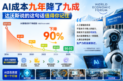
AI Costs Plummet by 90% Over Nine Years: Key Insights from Davos You Shouldn’t Miss
-
Doubao, Your Late-Night AI Companion, Now Eyes Profitability
-
![]()
SRC Empowers SEER Intelligence to Reach a Market Cap of Tens of Billions, Yet Fails to Sustain Profitability
-
![]()
China’s Embodied AI Industry Faces Fierce Domestic Competition, Making Overseas Expansion Essential for Survival
-
![]()
32.8 Billion Yuan Investment! Goertek’s 12-Inch AR Glasses Optical Wafer Base in Lingang Begins Operations
-
![]()
How Far is the All-New Li Auto L8 from Being the Best Five-Seat SUV with In-House Full-Stack Development?