Giants Enter the Market: Silicon Photonic Chips Herald New Opportunities
 04/25 2025
 636
636
Silicon photonic chips are a novel type of integrated circuit manufactured from silicon materials. They seamlessly integrate traditional electronic devices with optical devices, enabling the generation, transmission, modulation, and detection of optical signals. The core value of this technology lies in its ability to transcend the physical limitations of traditional electronic chips in terms of bandwidth, power consumption, and latency, thereby presenting a groundbreaking solution for the next generation of information technology.
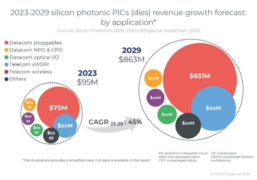
According to a Yole report, the market size of silicon-based photonic integrated circuits (PIC) was US$95 million in 2023 and is projected to soar to over US$863 million by 2029, exhibiting a compound annual growth rate (CAGR) of 45% from 2023 to 2029.
The evolution of silicon photonic chips dates back to the 1960s, when Bell Labs in the United States first introduced the concept of 'integrated optics'. However, for several decades thereafter, due to technological constraints and insufficient market demand, silicon photonic chips remained confined to laboratory settings. It was not until the advent of the 21st century, with the maturation of CMOS processes and the explosive growth in data center demand, that silicon photonic chips began to transition from theoretical research to industrial application. The involvement of tech giants like Intel and IBM further accelerated the rapid development of this technology.
In recent years, emerging scenarios such as AI large model training, high-performance computing, and 5G communication have imposed stringent demands on data transmission rates and energy efficiency ratios, further accelerating the technological advancement of silicon photonic chips. Industry insiders analyze that silicon photonics technology is gradually permeating from the high-end market to the consumer market, emerging as one of the most promising technological platforms following CMOS.
The silicon photonics industry encompasses a diverse array of participants, including major vertically integrated players actively engaged in the silicon photonics industry (e.g., Innolight, Cisco, Marvell, Broadcom, Coherent, Lumentum, Eoptolink); startups/design companies (e.g., Xphor, DustPhotonics, NewPhotonics, OpenLight, POET Technologies, Centera, AyarLabs, Lightmatter, Lightelligence, Nubis Communications); research institutions (e.g., UCSB, Columbia University, Stanford Engineering, MIT); foundries (e.g., Tower Semiconductor, GlobalFoundries, AMF (Advanced Micro Foundry), imec, TSMC, CompoundTek); and equipment suppliers (e.g., Applied Materials, ASML, Aixtron, ficonTEC, Mycronic Vanguard Automation, Shincron). These participants collectively contribute to significant growth and diversification within the industry.
Intel is among the earliest giants to delve into silicon photonics research, boasting over 30 years of experience in the field. Since the launch of its silicon photonics platform in 2016, Intel claims to have shipped over 8 million photonic integrated circuits (PICs) and over 3.2 million integrated on-chip lasers, with these products being adopted by numerous large cloud service providers.
Intel's silicon photonics technology leverages CMOS manufacturing processes to integrate optical devices such as lasers, modulators, and detectors with circuits on the same silicon substrate, thus realizing the integration of electronics and optics. It supports wavelength division multiplexing (WDM) technology, enabling a single optical fiber to simultaneously transmit optical signals of multiple wavelengths, along with efficient optoelectronic conversion technology, empowering silicon photonics modules to provide high-performance interconnectivity in scenarios like data centers.
Its previously launched 100G and 400G silicon photonics modules have achieved large-scale commercialization. Intel is collaborating with cloud computing giants and network equipment vendors to promote the standardization and popularization of silicon photonics technology.
At the Optical Fiber Communication Conference (OFC) in March last year, Intel showcased the Optical Computing Interconnect (OCI) chiplet, which packages a silicon photonics chip die and a CPU die together to form a system. The demonstration highlighted two CPUs communicating via optical fibers.
In this process, the OCI chiplet is responsible for converting the electrical signals of the CPU into optical signals. In a blog post, Intel mentioned that the fully integrated OCI chiplet based on its silicon photonics technology can achieve a bidirectional transmission rate of 4Tbps, supporting 64 data channels of 32Gbps in one direction within tens of meters, with the upper-layer protocol compatible with PCIe Gen 5.
Although this technology has not yet entered mass production, this demonstration clearly underscores the potential for the future development of silicon photonics integration technology. And Intel is not alone; in the past year, at least other upstream and downstream market participants, including NVIDIA and Synopsys, have begun to explore optical communication technology.
At last year's GTC conference, NVIDIA announced that TSMC and Synopsys would adopt NVIDIA's computational lithography platform for production to accelerate the manufacturing of and break through the physical limits of the next generation of advanced semiconductor chips.
TSMC and Synopsys have decided to integrate NVIDIA's cuLitho computational lithography platform into their software, manufacturing processes, and systems to expedite chip manufacturing and support the latest generation of NVIDIA Blackwell architecture GPUs in the future.
Jensen Huang stated, 'Computational lithography is the cornerstone of chip manufacturing. The cuLitho technology we have developed in collaboration with TSMC and Synopsys aims to apply accelerated computing and generative artificial intelligence to unlock new frontiers for semiconductor scaling.'
NVIDIA also introduced new generative AI algorithms that enhance the GPU-accelerated computational lithography library cuLitho, significantly improving semiconductor manufacturing processes compared to current CPU-based methods.
At this year's GTC conference, NVIDIA launched Spectrum-X Photonics, introducing an all-in-one packaged optical network switch to expand AI factories to millions of GPUs. Compared to traditional methods, they integrate optical innovation technology, reducing the number of lasers by 4 times, thereby achieving a 3.5-fold improvement in energy efficiency, a 63-fold improvement in signal integrity, a 10-fold improvement in large-scale network resilience, and a 1.3-fold improvement in deployment speed.
Jensen Huang remarked, 'AI factories are a new type of data center with ultra-large scale, and the network infrastructure must be thoroughly transformed to keep pace. By directly integrating silicon photonics technology into switches, NVIDIA is breaking the old limits of ultra-large-scale and enterprise networks and opening the door to AI factories with millions of GPUs.'
In the data communication market, Intel leads with a 61% market share, followed by Cisco, Broadcom, and other smaller companies. In the telecommunications sector, Cisco (Acacia) holds nearly 50% of the market share, followed by Lumentum (Neophotonics) and Marvell (Inphi), with coherent pluggable ZR/ZR+ modules driving the development of the telecommunications silicon photonics market. In the current market competition, Chinese vendors hold a relatively small share, but domestic companies such as Zhongji Xuchuang, Xinyisheng, Accelink, Bochuang Technology, Mingpu Optical Magnetics, and Hengtong Optic-Electric are beginning to participate, launching 400G, 800G, and even 1.6T silicon photonics modules. Zhongji Xuchuang's 1.6T silicon photonics module even employs self-developed silicon photonics chips and is in the market introduction phase.
In September last year, the Jiufengshan Laboratory successfully lit up the laser light source integrated into the silicon-based chip, achieving a domestic breakthrough in 'light-emitting chip' technology. This technology adopts a self-developed heterogeneous integration process, completing the process integration of indium phosphide lasers within an 8-inch SOI wafer, using optical signals to replace traditional electrical signals for high-speed transmission. This breakthrough not only signifies a new milestone in China's independent research and development capabilities in the field of silicon photonics chips but also lays the groundwork for large-scale commercialization in the future.
The industrialization process of silicon photonics chips is reshaping the power structure of the global semiconductor industry chain. The rapid transition from the laboratory to industrialization is attributed to several core driving forces.
The primary advantage of silicon photonics chips lies in their high compatibility with existing CMOS processes. Their core competitiveness stems from their seamless integration with existing semiconductor manufacturing processes. Traditional optical communication devices often necessitate complex discrete assembly processes, whereas silicon photonics chips can directly leverage existing wafer production lines for large-scale manufacturing through integration with CMOS processes. This compatibility not only significantly reduces production costs but also allows silicon photonics chips to seamlessly integrate into existing semiconductor supply chains.
Moreover, the introduction of new material systems offers more possibilities for the functional expansion of silicon photonics chips. The incorporation of materials such as indium phosphide (InP) and lithium niobate (LiNbO3) compensates for the deficiency of silicon as a light-emitting material, further enhancing the performance of the chip.
With the surging demand for artificial intelligence, big data, and high-performance computing, the limitations of traditional electronic chips in terms of bandwidth, power consumption, and latency are gradually becoming apparent. Especially in AI large model training and inference scenarios, the processing requirements for massive amounts of data pose unprecedented challenges to the computing power and energy efficiency of chips. Silicon photonics chips, with their high bandwidth, low latency, and high energy efficiency ratio characteristics, have emerged as a pivotal tool to address these challenges.
Data centers are among the most crucial application scenarios for silicon photonics chips. According to statistics, the data traffic generated by global data centers has reached the Zettabyte level annually. Traditional copper cable connections face severe signal attenuation issues in long-distance transmission, whereas optical fiber communication, despite its high bandwidth advantage, is hindered by high costs in large-scale adoption. By integrating the photoelectric conversion function onto a single chip, silicon photonics chips retain the high-bandwidth characteristics of optical fiber communication while significantly reducing system complexity and deployment costs. Taking 800G optical modules as an example, products utilizing silicon photonics technology can save approximately 30% of power consumption compared to traditional solutions, while reducing volume by over 40%. These advantages make them the preferred solution for cloud computing vendors and telecom operators.
Although silicon photonics chips were initially predominantly used in high-end markets such as data centers and long-distance communications, with the maturation of technology and the reduction of costs, their application scenarios are rapidly expanding into multiple emerging fields. Silicon photonics technology is gradually becoming a core driving force for breakthrough innovations in intelligent driving, optical computing, and consumer electronics.
In the realm of intelligent driving, the silicon photonics solid-state LiDAR technology route is considered the key to achieving large-scale commercialization. Currently, LiDAR primarily relies on discrete device integration, facing bottlenecks such as high cost, large size, and inadequate power consumption and reliability. The silicon photonics chip-based solution significantly reduces system complexity and manufacturing costs through high-density integration compatible with CMOS processes. Specifically, the two solid-state LiDAR solutions, silicon-based phased arrays, and optical switch arrays, are driving the evolution of LiDAR from mechanical to fully solid-state due to their miniaturization and anti-vibration characteristics.
Mobileye's silicon photonics LiDAR SoC (System-on-Chip) adopts frequency-modulated continuous wave (FMCW) technology and is scheduled for launch this year. This solution integrates multiple laser emission, reception, and signal processing units onto a single silicon-based chip, reducing the volume to 1/10 that of traditional mechanical radars while lowering the cost to the hundreds of dollars range, meeting automotive-grade reliability requirements.
Furthermore, the potential of silicon photonics technology in the field of optical computing is also attracting considerable attention. Amidst the surging demand for computing power and the prominence of the energy efficiency bottleneck in traditional electronic computing, optical computing, with its advantages of parallel processing, low power consumption, and anti-interference, has emerged as a cutting-edge direction to overcome the limitations of the von Neumann architecture. Relying on mature semiconductor processes, the silicon photonics platform can achieve nanoscale integration of core components such as optical waveguides and modulators, providing a high-density, programmable hardware foundation for optical quantum computing chips. Silicon-based waveguides can stably generate and manipulate photon entangled states, while programmable optical switch arrays support efficient routing of quantum states. Research indicates that silicon photonics chips have achieved 128-mode Gaussian boson sampling, with an integration density 50 times higher than discrete device solutions, verifying their feasibility in qubit expansion. This progress is regarded as a significant milestone toward the practical application of optical quantum computing.
In the realm of consumer electronics, silicon photonics technology's high integration characteristics align seamlessly with the trend towards miniaturizing devices. Wearable devices and biomedical sensors, among other applications, demand stringent space utilization, and silicon photonics chips excel in integrating light sources, detectors, and signal processing units within micrometers, thus substantially enhancing functional density. Their adoption in areas such as miniaturized spectral analysis and health monitoring is steadily transitioning from laboratory settings to commercial realms. The optical module developed by Meta in collaboration with silicon photonics chip manufacturers exemplifies this, reducing image transmission power consumption by 40% while supporting 8K resolution output through the seamless integration of silicon photonics modulators and waveguides. This interdisciplinary technological advancement signifies a significant leap for silicon photonics, transitioning from single-chip manufacturing to system-level solutions.
This technological revolution, which substitutes photons for electrons, not only represents a groundbreaking innovation for the traditional semiconductor industry but also paves the way for the 'optoelectronic fusion era'. Looking ahead, the industrialization journey of silicon photonics chips encounters numerous challenges. How can we manage thermal effects while enhancing integration? What strategies can we employ to achieve superior heterogeneous integration of III-V materials with silicon-based processes? Can we overcome the scalability limitations of optical quantum computing? The resolution of these questions will undoubtedly shape the depth and breadth of the ongoing technological evolution.
-
![]()
The First Batch of Victims of the AI Bubble: Programmers
-
![]()
ByteDance, DJI, and Xiaohongshu Secure Top Three Positions Among China’s Fastest-Growing Unicorns
-
Tesla's in-car voice system in China is finally learning to 'understand human language'
-
![]()
Foreigners Are Amazed: Chinese Electric Vehicle Drive Systems Unveil Innovative 'Poses'
-
![]()
700,000 Brothers and the Future of Robots: Behind JD.com's 'Nirvana Plan'
-
![]()
Zhipu's Trillion-Dollar Valuation: A New Chapter for China's AI
-
![]()
Is Laifen, a 'Dyson Alternative' on the Rise, Now Ensnared by the 'Alternative Curse'?
-
![]()
Beyond Patents: Insta360 and DJI Compete in Retail