AI Chip "Power Cliff": Revolutionizing Cooling Technology for Large Models
 05/03 2025
 841
841

The power consumption and heat generation of AI chips profoundly impact a company's costs, risks, and the chips' stability and longevity. Frequent overheating or short circuits can severely diminish the effectiveness and efficiency of AI training and inference processes.
A revolution in cooling technology is urgently needed.
Statistics reveal that global data volume stood at around 10EB (Exabytes) in 2015 and is projected to soar to 175ZB (Zettabytes) by 2025, potentially reaching an astonishing 2432ZB by 2035. However, edge AI faces two significant challenges. First, balancing performance, power consumption, and cost is crucial. Enhancing computational power without pushing power consumption and cost to unreasonable limits, especially in battery-powered low-power devices, is essential. Second, building a robust ecosystem encompassing toolchains, languages, compatibility, and ease of development is vital for the popularization and large-scale application of AI technology, similar to the development of CPUs and GPUs.
ChatGPT and similar AI robots utilizing large language models (LLMs) to generate human-like conversations are just one of many new AI applications reliant on "parallel computing." This term refers to a network of chips performing massive computational tasks simultaneously.
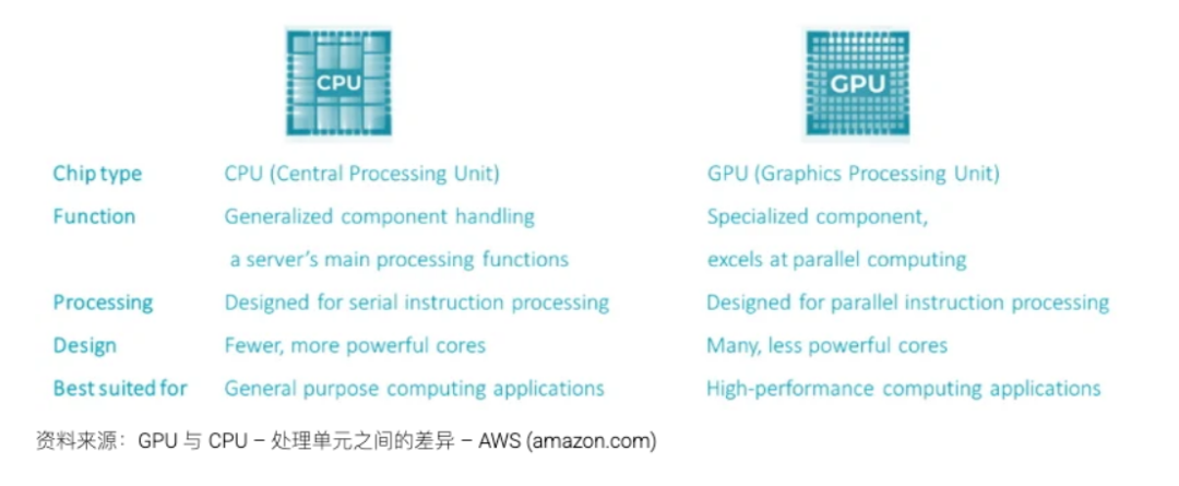
At the heart of AI infrastructure lies the GPU (Graphics Processing Unit), excelling in handling specialized high-performance parallel computing tasks required for AI. Compared to the CPU (Central Processing Unit) used in personal computers, this robust processing capability comes at the cost of higher energy input and, consequently, greater heat output.
High-end GPUs exhibit a power density approximately four times that of CPUs, posing significant challenges for data center planning. The originally calculated power is now only 25% of what is required to run modern AI data centers. Even cutting-edge hyperscale data centers used by Amazon, Microsoft, and Alphabet for cloud computing are still CPU-driven. For instance, Nvidia's current A100 AI chip consumes approximately 400W per chip, while its latest microchip, the H100, consumes nearly twice as much, reaching 700W, akin to a microwave oven's power consumption. If a hyperscale data center with an average of one million servers replaces its current CPU servers with these GPUs, the required power will increase by 4-5 times (1500MW), equivalent to a nuclear power plant!
The increase in power density means that the heat generated by these chips will also surge. Hence, cooling systems must be more robust. Such changes in power and cooling will necessitate an entirely new design for future AI-driven data centers, leading to a significant supply and demand imbalance in underlying chips and data center infrastructure. Considering data center construction timelines, industry experts predict that we are in the early stages of a decade-long modernization upgrade aimed at making data centers more intelligent.
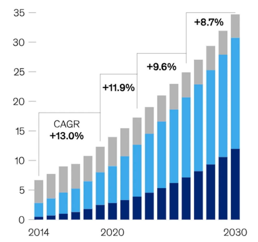
Growth in Electricity Consumption by U.S. Data Centers (Gigawatts)
TSMC's 3DVC (3D Vapor Chamber) technology represents an advanced thermal solution for high-performance computing (HPC) and AI chips, addressing the surge in power consumption and heat generation density caused by increased integration in advanced process nodes (such as 3nm/2nm) chips.
Unlike traditional vapor chambers with a two-dimensional planar structure, TSMC's 3DVC integrates multiple layers of microfluidic channels directly within the chip package through a three-dimensional design, utilizing phase change heat transfer (liquid evaporation-condensation cycle) to rapidly export heat.
Key features include:
- Three-dimensional capillary structure: Uses porous metal foam or micro-pillar arrays internally to enhance the capillary reflow capacity of the working fluid (such as water/ammonia).
- Near-junction cooling: Directly contacts the chip's silicon interposer or 3D stacked structure (such as SoIC) to shorten the heat conduction path.
The heat pipe in a 3D-VC heat sink is a one-dimensional linear heat transfer device. Conventional VC vapor chambers have an evaporation section and a condensation section, and depending on the design location, there are multiple possible heat dissipation path distributions, making them two-dimensional heat transfer devices. However, their heat dissipation paths are still limited to the same plane. In contrast, the heat conduction path of a 3D-VC heat sink is three-dimensional, stereoscopic, and non-planar. The 3D-VC heat sink leverages a combination of VC and heat pipes to connect internal chambers, enabling working fluid reflow and heat conduction through the capillary structure. The connected internal chambers and welded fins form the entire cooling module, facilitating multi-dimensional heat dissipation, such as horizontally and vertically.
The multi-dimensional heat dissipation path allows the 3D-VC heat sink to contact more heat sources and provide more heat dissipation paths when managing heat generated by high-power devices. In traditional cooling modules, heat pipes and VC vapor chambers are separately designed, leading to suboptimal cooling due to increased thermal resistance with longer heat conduction distances. The 3D-VC heat sink extends the heat pipe into the body of the VC vapor chamber, connecting the vacuum chamber of the VC vapor chamber with the heat pipe, integrating the internal working fluid, and placing the 3D-VC heat sink in direct contact with the heat source. The vertical heat pipe design also enhances heat transfer speed.
3DVC can be embedded in TSMC's CoWoS 2.5D/3D packaging, offering integrated cooling for CPU/GPU/HBM. TSMC demonstrated a 3DVC prototype at the IEEE International Electron Devices Meeting (IEDM), reducing the junction temperature of a 3nm chip by over 15°C. It is planned to be applied to the next-generation products of AMD and NVIDIA simultaneously with the CoWoS-L packaging technology.
Liquid cooling is the only viable solution at high power levels.
The efficiency of heat transfer through the flow of a certain volume of liquid is significantly higher than that of air—water is approximately 3,600 times more efficient. This makes liquid cooling through chip heat sinks an efficient method. When the heat dissipation per square centimeter of chip area exceeds approximately 50 watts, liquid cooling is typically required. Given that the area of GB200 is roughly 9 square centimeters, any heat dissipation exceeding 450 watts necessitates pumped liquid cooling. In "direct chip" cooling, the liquid flows through cold plate channels connected to the chip heat sink via a thermal interface. When the liquid does not evaporate during this process, it is termed "single-phase" operation, where the medium (usually water) is pumped through a fan-cooled heat exchanger. Flex's subsidiary JetCool offers direct chip liquid cooling modules that use a small array of fluid jets precisely targeted at hot spots on the processor, thereby enhancing high-power electronic cooling performance at the chip or device level.
Heat can be transferred to a second liquid loop, providing hot water for buildings and potentially local consumers. Two-phase operation offers superior heat transfer by causing the liquid (typically a fluorocarbon) to evaporate when absorbing heat and then recondense at the heat exchanger, significantly boosting performance. However, system fans are still necessary to cool other components, though some components (like DC/DC converters) can be integrated into the liquid cooling loop using their own substrates, aligning with the concept of "vertical power delivery," where the DC/DC converter is positioned directly below the processor to minimize voltage drop. The practical limitation of the direct chip approach lies in the thermal resistance at the interface between the chip and the cooling plate, necessitating precise surface flatness and high-performance solder paste. However, at kilowatt-level powers, temperature differences remain a concern.
To address this limitation, immersion cooling technology can be considered. The entire server is submerged in an open dielectric fluid tank, with the dielectric fluid pumped through a loop from a reservoir to a heat exchanger. Similarly, for optimal performance, two-phase operation can be employed.
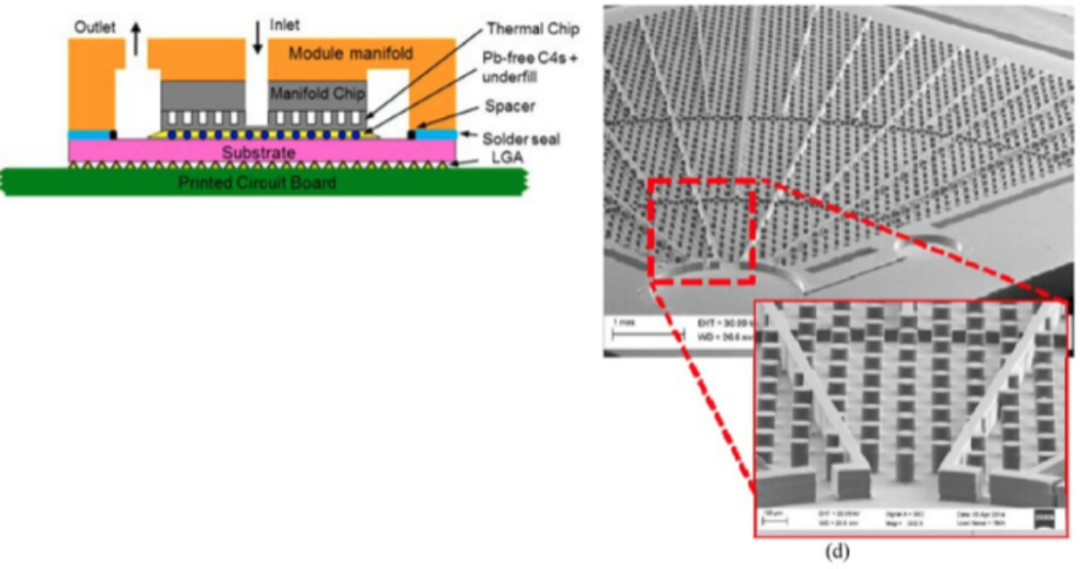
IBM employs embedded microchannel phase change cooling technology, another innovative approach. IBM pumps the dielectric fluid directly into microscopic gaps of approximately 100μm in any level of chip stacking, extracting heat from the chip through the boiling of the dielectric fluid from liquid to gas phase. They tested a modified IBM Power 7+ chip with this technology, resulting in a 25°C reduction in junction temperature.
To achieve embedded cooling, IBM removed the processor's package lid to expose the die, performed deep reactive ion etching (DRIE) on the die, constructed 120μm deep cooling channel structures on its back, and bonded a glass plate to the etched chip to form the top wall of the microchannels. Adhesive was used to bond the coolant inlet and outlet brass manifolds to the glass manifold chip and organic substrate. The coolant enters the module and is distributed through 24 inlets into the corresponding 24 radially expanding channels.
NVIDIA: Hardware-Level Cooling Integration (NVLink C2C Technology)
The release of Blackwell heralds a new era in AI hardware, providing unprecedented computational support with its powerful performance, enabling the training of more complex and precise models. AI computing power based on Blackwell is offered to users through a complete server called DGX GB200, which integrates 36 NVIDIA Grace CPUs and 72 Blackwell GPUs. These superchips are connected into a supercomputer via the fifth-generation NVLink, enhancing overall computing performance. To better support the application of GB200 superchips, NVIDIA has introduced a new computing cluster, the DGX GB200 SuperPod. This supercomputing cluster adopts a novel and efficient liquid-cooled rack-scale architecture, offering astonishing computing power and memory capacity at FP4 precision. Through the DGX GB200 SuperPod, NVIDIA will empower various industries with robust AI computing capabilities, supporting the AI industrial revolution and once again demonstrating its leadership and innovation in the field.
Specifically, NVLINK is a high-speed interconnect technology designed to connect NVIDIA GPUs. It allows GPUs to communicate in a point-to-point manner, bypassing the traditional PCIe bus, achieving higher bandwidth and lower latency. NVLINK can connect two or more GPUs for high-speed data transfer and sharing, offering enhanced performance and efficiency for multi-GPU systems.
For instance, the GB200 NVL72 comprises 18 1U servers, delivering 720 petaflops of FP8 performance and 1440 petaflops of FP4 computing performance, capable of handling up to 27 trillion AI LLM parameter models. Each server contains two GB200 Grace Blackwell Superchips, and these compute nodes feature 1.7TB of HBM3E memory and 32TB/s of memory bandwidth. To address excessive power consumption, NVIDIA has opted for liquid-cooled MGX packages and adopted a liquid-cooled rack-level solution.
-
![]()
ByteDance, DJI, and Xiaohongshu Secure Top Three Positions Among China’s Fastest-Growing Unicorns
-
Tesla's in-car voice system in China is finally learning to 'understand human language'
-
![]()
Foreigners Are Amazed: Chinese Electric Vehicle Drive Systems Unveil Innovative 'Poses'
-
![]()
700,000 Brothers and the Future of Robots: Behind JD.com's 'Nirvana Plan'
-
![]()
Zhipu's Trillion-Dollar Valuation: A New Chapter for China's AI
-
![]()
Is Laifen, a 'Dyson Alternative' on the Rise, Now Ensnared by the 'Alternative Curse'?
-
![]()
Beyond Patents: Insta360 and DJI Compete in Retail
-
![]()
Piercing Through Industry Chaos: The Curtain Rises on Compliance for Autonomous Driving