65-Year-Old Overseas Returnee Master Creates Unicorn Enterprise: Providing Semiconductor "Physical Examination" Services, the Only One in China
 08/11 2025
 730
730
In today's world, where smartphones, tablets, smart TVs, and even car central control screens are omnipresent, have you ever wondered how these precise and smooth screens and powerful internal chips ensure flawless production?
Behind this lies a type of sophisticated "eye" known as Automatic Optical Inspection (AOI) equipment.
Zhongdao Optoelectronics is leveraging its self-developed "penetrating eyes" to promptly identify issues in the production process of "Chinese screens" and "Chinese chips".
Recently, this hidden champion in pan-semiconductor inspection equipment from Zhaoqing, Guangdong, has registered for counseling and filing with the Guangdong Securities Regulatory Bureau, officially initiating the A-share listing process.
In 2016, it was listed on the New Third Board, becoming the only semiconductor equipment company in China to achieve commercialization and list on the New Third Board; in March 2021, it voluntarily terminated its listing.
The flat panel display and semiconductor inspection industry to which Zhongdao Optoelectronics belongs presents the following new opportunities:
1. Semiconductor inspection: domestic substitution demand
The Chinese integrated circuit market is growing rapidly, yet domestic inspection equipment penetration remains low (only 8% in 2022). With policy support, there is significant room for domestic substitution.
Advancements in chip process technology (such as 5nm, GAAFET, MRAM) increase inspection demand, and the market potential for high-end inspection equipment is substantial.
2. Flat panel display inspection: technological upgrading opportunity
The global market for inspection equipment for new display devices is growing rapidly, with a significant market share in China, and is expected to continue growing at a high rate until 2030.
New display technologies such as OLED, Micro-LED, and Mini-LED have strong demand for high-precision inspection equipment.
3. New application areas
AI inspection systems (based on deep learning) improve efficiency, with an accuracy rate exceeding 99%, and market growth is expected to exceed 30% over the next five years.
Demand in the automotive electronics sector is surging, with smart car chips and in-vehicle display screens requiring high-precision inspection; the rise of AR/VR and the metaverse necessitates high-resolution display inspection equipment.
- 01 -
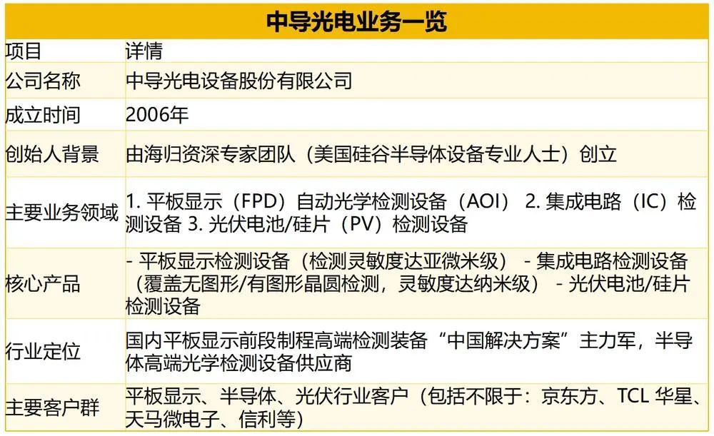
The founder of Zhongdao Optoelectronics Equipment Co., Ltd. (hereinafter referred to as "Zhongdao Optoelectronics") is Li Bo.
Li Bo graduated from the Department of Physics, Semiconductor Major at Wuhan University, and was among the earliest university graduates to systematically study semiconductor technology. He later pursued further studies in the United States, earning two master's degrees in Electronic Engineering and Business Administration from Santa Clara University.
In 1994, he officially entered the semiconductor industry, working for KLA-Tencor, a renowned American company. During this time, he not only participated in the development of multiple key technologies but also led a team in successfully developing the world's first dark-field structured wafer inspection equipment.
In 2006, Li Bo, nearing his fifties, led a dozen semiconductor elites from Silicon Valley back to China. They jointly founded Zhongdao Optoelectronics in Zhaoqing, Guangdong, focusing on providing high-end automatic optical inspection equipment for the semiconductor and flat panel display industries, aiming to break the long-term monopoly of foreign enterprises in this field.
Currently, Zhongdao Optoelectronics is the only supplier in mainland China capable of providing sub-micron level inspection equipment for the front-end process of flat panel displays.
- 02 -
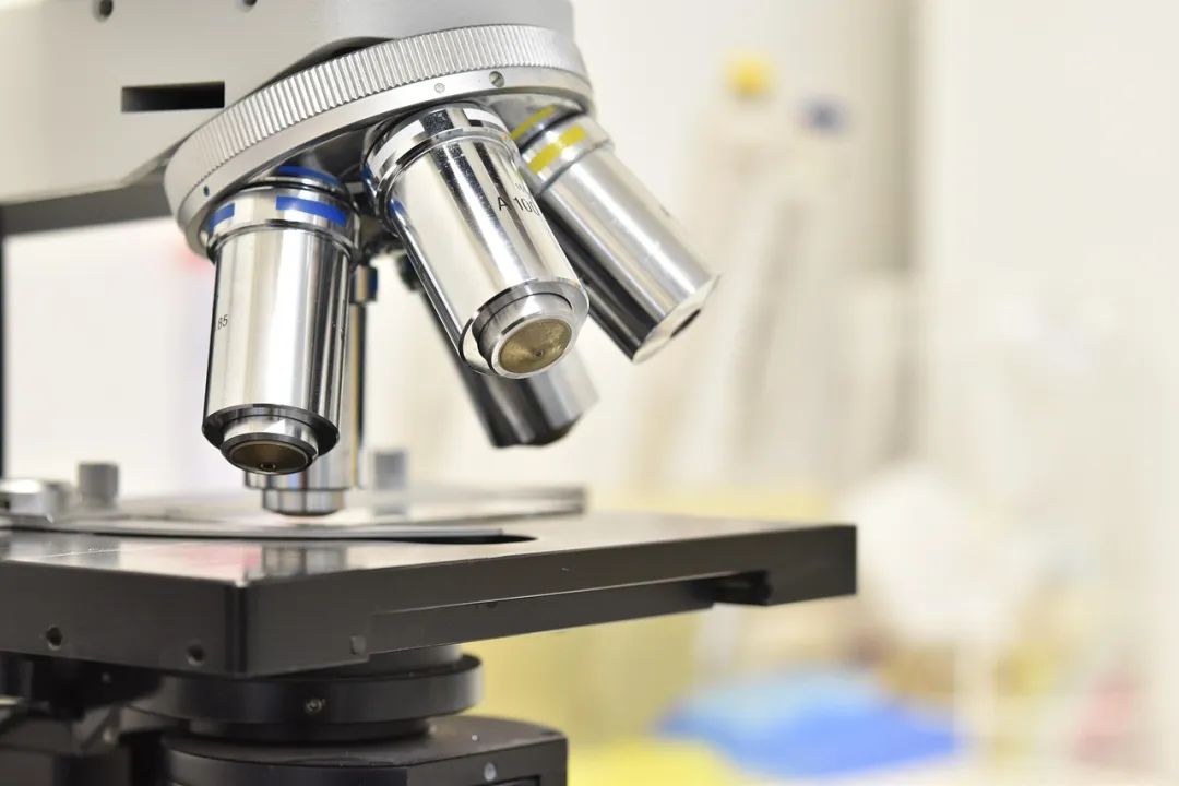
Zhongdao Optoelectronics' equipment is akin to high-tech instruments performing "physical examinations" on chips and display screens, ensuring the quality and stability of these core components.
Their business primarily focuses on three areas: semiconductor chip inspection, flat panel display inspection, and photovoltaic cell/wafer inspection.
Among them, semiconductor chip inspection is their flagship business, flat panel display inspection is the core pillar, and photovoltaic inspection serves as a supplementary business supporting the new energy sector.
Zhongdao Optoelectronics' "signature skill" lies in high-end automatic optical inspection equipment. These devices act as "quality inspectors" in semiconductor and flat panel display manufacturing, responsible for identifying defects too small to be detected by the naked eye, ensuring that every chip and screen meets high standards.
- Flat panel display inspection: sub-micron level "penetrating eyes"
In the field of flat panel displays (such as common LCD and OLED screens), Zhongdao Optoelectronics' inspection equipment has formed a comprehensive product family that covers all aspects, from the initial stage of screen manufacturing and glass substrate to the final product.
Their equipment boasts sub-micron level sensitivity, meaning it can detect defects millions of times smaller than a hair strand, such as minute scratches on the screen, particle contamination, or circuit breaks.
Imagine an OLED screen for a mobile phone. During production, it may develop minor flaws due to dust or process deviations. If these flaws are not detected, the screen may experience uneven display, color differences, or even be scrapped directly.
Zhongdao Optoelectronics' equipment functions like a super microscope, utilizing laser and optical technology to scan the screen surface and accurately locate issues, ensuring that every screen meets high-quality standards. This high precision makes Zhongdao Optoelectronics the "main force" in front-end process inspection for flat panel displays in China.
- Semiconductor inspection: nanometer-level "precise hunters"
In the semiconductor field, Zhongdao Optoelectronics' equipment covers two major application scenarios: unpatterned wafer inspection and patterned wafer inspection.
Unpatterned wafer inspection is primarily used to inspect bare silicon wafers or wafers without patterns, such as in the certification process before wafers leave the factory or enter the production line. This type of inspection employs laser scanning of the wafer surface to capture defects like particle contamination, scratches, and watermarks, with a sensitivity of nanometer level, capable of detecting flaws smaller than bacteria.
Patterned wafer inspection is more complex, targeting wafers that have already been etched with circuit patterns. This type of inspection requires the equipment to distinguish true defects from normal circuits in intricate patterns.
Through multi-channel laser scattering technology and intelligent algorithms, Zhongdao Optoelectronics' equipment accurately differentiates defect signals and has successfully entered the production lines of domestic wafer fabs, safeguarding chip manufacturing.
Against the backdrop of the long-term monopoly of the global semiconductor equipment market by American and Japanese companies (such as KLA and Hitachi High-Tech), Zhongdao Optoelectronics has broken through technical barriers through independent research and development, providing "Chinese solutions" and reducing domestic enterprises' dependence on imported equipment.
This localization advantage not only makes the equipment more suited to the needs of Chinese customers but also more competitive in terms of cost and after-sales service.
- 03 -
The semiconductor and flat panel display inspection equipment industry in which Zhongdao Optoelectronics operates is witnessing its potential being continuously tapped.
1. Semiconductor inspection: urgent need for domestic substitution
According to industry data, the global semiconductor inspection equipment market was approximately $13.1 billion in 2020 and is expected to achieve a compound annual growth rate (CAGR) of 14% over the next five years, far exceeding the global average.
However, the penetration rate of domestic inspection equipment remains low. Taking Huahong Wuxi and Jita Semiconductor in 2022 as examples, the localization rate of metrology equipment was only 8%, far lower than other types of equipment.
This low localization rate represents an opportunity for the semiconductor inspection industry. For example, Zhongdao Optoelectronics' nanometer-level inspection equipment fills the gap in China's high-end inspection field and is expected to achieve mass shipments in the future with the expansion of wafer fabs and the wave of localization.
In addition, the continuous advancement of chip process technology has also increased inspection demand.
As the chip process shrinks from 45nm to 5nm, the number of process steps increases from approximately 430 to 1250, each requiring precise inspection to avoid defects. New technologies such as GAAFET (gate-all-around field-effect transistor) and MRAM (magnetic random-access memory) further increase inspection difficulty.
2. Flat panel display inspection: "frontier" of display technology upgrading
The flat panel display industry also boasts a bright future. LCD and OLED screens are core components of smartphones, TVs, laptops, and other products.
In 2024, the global market size for inspection equipment for new display devices is expected to reach billions of yuan and is anticipated to continue growing at a high CAGR until 2030, with a significant market share in China.
China occupies an important position in the global flat panel display industry. According to market data, China's flat panel display inspection equipment market accounted for a large proportion of the global market in 2022, and the CAGR over the next few years is expected to be higher than that of the United States and Europe.
This is because China has the world's largest display panel production capacity, with companies such as BOE and TCL Huaxing ranking among the top globally. These panel giants have strong demand for high-precision inspection equipment, providing a stable local market for the flat panel display inspection industry.
Simultaneously, the upgrading of display technology brings new opportunities.
OLED screens are gradually replacing LCD screens due to their flexibility and high contrast, while new display technologies such as Micro-LED and Mini-LED are also on the rise. These new technologies have higher requirements for the precision and flexibility of inspection equipment.
3. Opportunities from industrial transfer
The global semiconductor and flat panel display industries are experiencing a third wave of capacity transfer, with the focus gradually shifting to mainland China. China is not only the world's largest semiconductor consumer market but is also actively expanding wafer fabs and panel production lines.
For instance, giants such as TSMC and Samsung are investing and building factories in China, while local enterprises such as SMIC and Yangtze Memory Technologies are also accelerating their expansion. These new production lines require a substantial amount of inspection equipment, creating vast market space for domestic inspection equipment manufacturers.
4. Explosion of new application areas
The rapid development of artificial intelligence technology is bringing revolutionary changes to the inspection industry.
Traditional inspection methods primarily rely on manual visual inspection and simple algorithms, but they are inadequate when facing nanometer-level defects.
Now, AI inspection systems based on deep learning can complete defect analysis of high-resolution images within milliseconds, with an accuracy rate exceeding 99%, far surpassing manual inspection levels.
What is more noteworthy is that the massive amounts of data accumulated by inspection equipment are becoming valuable assets. Through big data analysis, companies can not only achieve predictive maintenance of equipment but also optimize production processes, fundamentally improving product yield.
Currently, the application of AI in the inspection industry is still in its infancy, and market growth is expected to exceed 30% over the next five years, which will bring new profit growth points for equipment manufacturers.
The automotive electronics sector deserves particular attention. The demand for smart car chips is several times that of traditional cars, and in-vehicle display screens (such as central control screens and dashboards) also require high-precision inspection equipment.
Additionally, the rise of AR/VR and the metaverse also brings new demand for flat panel display inspection. AR glasses require high-resolution, lightweight display screens, making inspection more challenging.
- 04 -
Despite numerous opportunities, the entire industry also faces some challenges.
The global semiconductor inspection equipment market is still dominated by giants such as KLA from the United States (with a market share of about 51%) and Hitachi High-Tech from Japan, and the technical barriers are extremely high.
Secondly, cyclical fluctuations in the semiconductor industry may affect equipment demand, especially during economic downturns.
But overall, the semiconductor and flat panel display inspection industry is ushering in a golden age of development.
Driven by the four forces of domestic substitution, technological upgrading, AI empowerment, and policy support, this sub-sector is expected to maintain sustained and rapid growth.
For local enterprises like Zhongdao Optoelectronics, as long as they can break through high-end technological barriers, they have the opportunity to occupy an important position in the global inspection equipment market.
This article does not constitute any investment advice.
-
On the Eve of Its IPO, Avatr Finds Itself Embroiled in a 'Farce of Controversy and Belittlement'
-
![]()
Yutong Optics' Japanese Subsidiary Unveiled in Tokyo, Shifting Strategic Focus to Technology-Driven Growth
-
![]()
Half-Year Revenue Outstrips Last Year’s Total! Zhongrun Optics Forecasts 80.2% H1 Revenue Growth
-
![]()
Why Does AI Competition Start with Computing Power?
-
![]()
Apple AI Finally Makes Its Debut in China, Yet iPhone's 'AI Autonomy' Faces Uncertainty
-
![]()
Apple AI and QianWen Make Up Lessons: Alibaba Has Its Own 'Doubao Phone'
-
![]()
QianWen Joins Apple, Signal for Large Models to ‘Fade into the Background’
-
![]()
The ‘Anchor’ Strategy of Google Hidden Behind the Bleeding Financial Report