Advancements in Ultrafast Nonlinear Optical Techniques: On-chip Femtosecond Pulse Amplification
![]() 01/13 2025
01/13 2025
![]() 879
879
On-chip integrated femtosecond lasers hold immense potential for applications in real-time diagnosis, biomedical imaging, portable chemical sensing, and radar navigation. However, due to the narrow widths of integrated waveguides, typically on the order of hundreds of nanometers, optical pulses undergo significant nonlinear phase shifts during amplification, leading to pulse distortion and potential device damage. To overcome this challenge, a research team from the University of Hamburg, Germany, drew inspiration from chirped pulse amplification technology (CPA) and achieved a remarkable 50-fold amplification of 1 GHz chirped pulses on a CMOS-compatible photonic chip, with a peak power of 800 W and a pulse width of 116 fs [1].
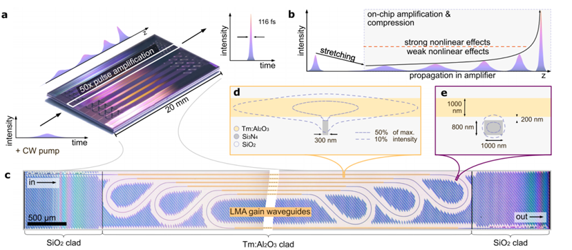
Figure 1: Schematic representation of on-chip ultrafast pulse amplification [1]
The process of on-chip femtosecond pulse amplification is depicted in Figure 1a: A signal light of 1.81 mW with a central wavelength of 1815 nm and a repetition frequency of 1 GHz is coupled into the amplifier and pumped by continuous light at 1610 nm in the thulium-doped alumina gain layer. This results in the final output of 116 fs pulses with an energy of 95 pJ and a spectral bandwidth of 3.5 THz. Figure 1b illustrates the pulse evolution during amplification, where the broadened pulse primarily undergoes linear transmission in the amplifier waveguide, with nonlinear effects becoming significant only towards the end of the transmission. For compact integration, as shown in Figure 1c, the total length of the amplifier waveguide structure is 12 cm, comprising approximately 10 cm of straight waveguide segments providing gain and around 2 cm of curved waveguide segments. The straight and curved waveguides are seamlessly connected by a tapered waveguide, with the optical mode field distributions at different positions displayed in Figures 1d and 1e, respectively.
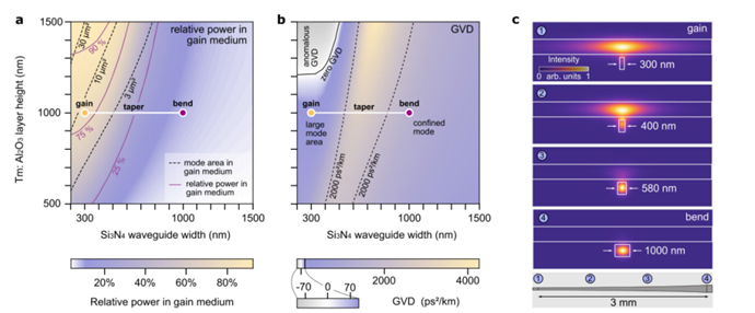
Figure 2: Design schematic of the amplifier [1]
By meticulously designing the size parameters of the amplifier, such as the width of the silicon nitride waveguide and the height of the thulium-doped alumina gain layer (as shown in Figure 2a), the optical field is concentrated primarily within the gain layer during amplification in the straight waveguide segment, maximizing energy extraction. As the light propagates through the curved waveguide, the optical field is predominantly distributed within the waveguide to minimize transmission loss. Furthermore, as depicted in Figure 2b, by fine-tuning the system parameters, full positive group velocity dispersion is achieved throughout the amplifier structure, enabling efficient pulse compression. Figure 2c illustrates the evolution of the optical mode field distribution in the tapered waveguide that connects the straight and curved waveguides.
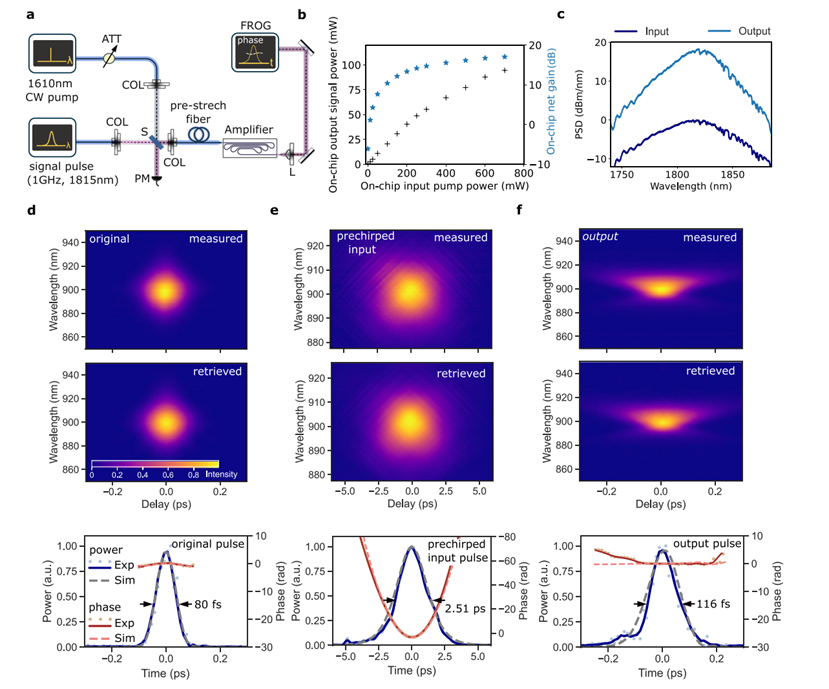
Figure 3: Experimental test results of the amplifier [1]
After successfully fabricating the chip, the research team set up a test optical path as shown in Figure 3a and employed the FROG method to measure the time-domain characteristics of the output pulse. At a chip pump power of 700 mW, the output pulse power reached 95 mW, with a gain of approximately 17 dB. Figures 3d, 3e, and 3f present the FROG measurement and reconstruction diagrams of the original pulse, chirped pulse, and output pulse, respectively. Observing Figure 3f, it is evident that the output pulse exhibits a weak residual third-order dispersion, which the research team attributes to the limited gain bandwidth and nonlinear phase accumulation during amplification. In summary, this study demonstrates a 50-fold amplification of 1 GHz femtosecond pulses on a CMOS-compatible photonic chip with a peak power of 800 W, achieved through the optimized design of a large-mode-field gain waveguide. This research paves the way for large-scale, high-power on-chip integrated ultrafast light sources, fostering further advancements in on-chip photonics.
References:
[1] Gaafar M A, Ludwig M, Wang K, et al. Femtosecond pulse amplification on a chip[J]. 2023. DOI:10.1038/s41467-024-52057-3.

