Photonics Technology Propels AI Transformation in Data Centers: Journey from Fiber Optic Connectivity to Co-Packaged Optics
 05/12 2025
 975
975
Produced by ChiNengZhiXin
At the Optical Fiber Communication Conference (OFC) 2025, industry pioneers concurred that photonics technology is emerging as the linchpin in interconnecting AI computing powerhouses within data centers. As large language models (LLMs) necessitate unprecedented computational prowess and bandwidth, traditional electrical interconnects struggle to support the escalating expansion of future AI clusters.
Commencing with an overview of the photonic component market and the AI-driven evolution of interconnect demands, we delve into the applications and hurdles of optical interconnects within two primary network architectures: "Scale-Out" and "Scale-Up." Additionally, we spotlight how co-packaged optics (CPO) technology achieves breakthroughs in power efficiency, bandwidth, and reliability.
Looking ahead, with the concerted efforts of AI data center operators and chip giants, photonics technology is transitioning from being "optional" to "indispensable," poised to fundamentally reshape the interconnect landscape in data centers.
Part 1
AI-Driven Explosion in Data Center Interconnect Demands
Photonics Component Market: A Shift from Telecommunications to Data Communications
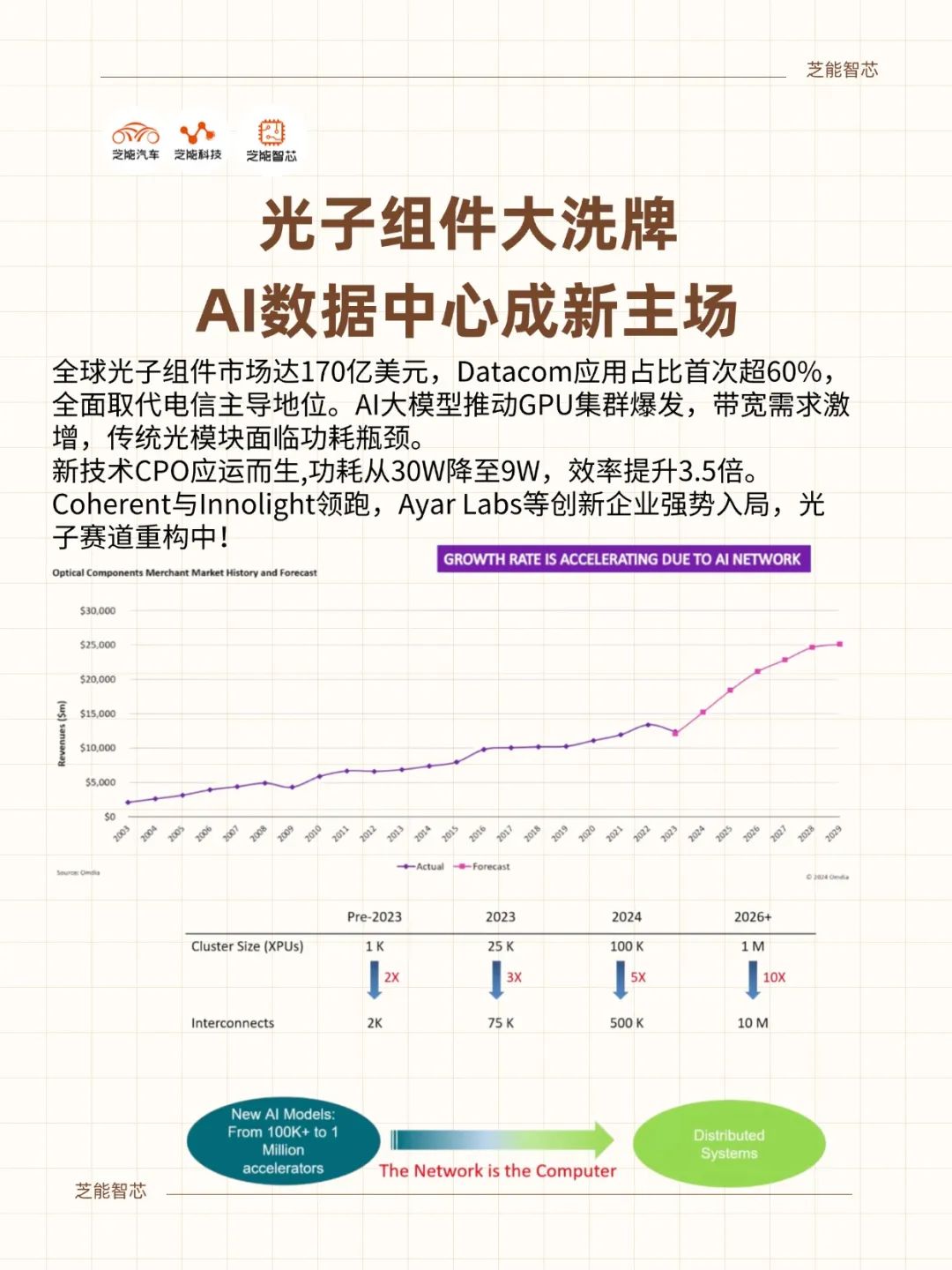
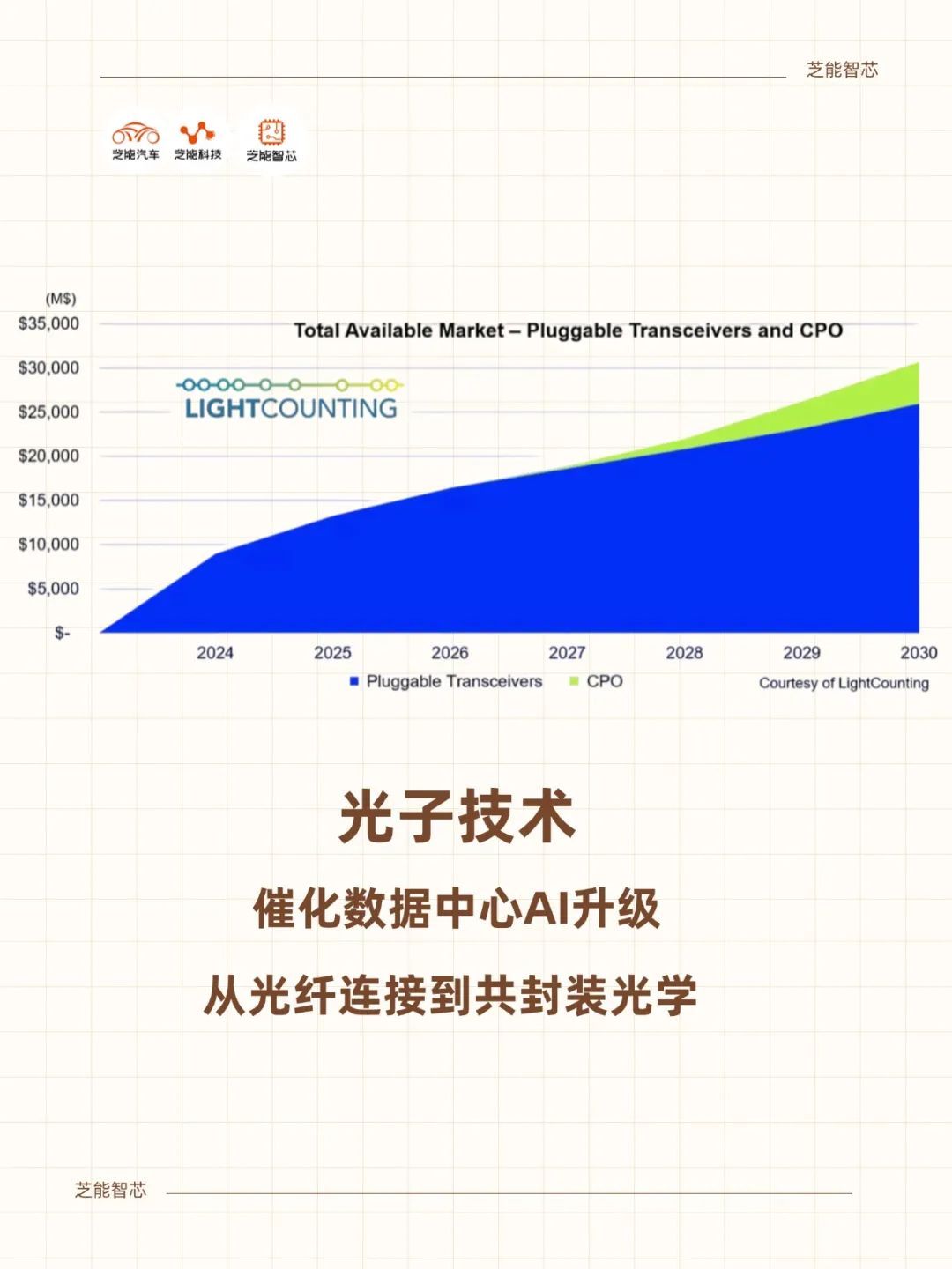
In 2024, the global photonic component market was estimated at roughly $17 billion, traditionally dominated by telecommunications applications. However, as the need for high-bandwidth, low-latency interconnects in AI data centers skyrockets, the market is undergoing a structural transformation: the share of data communications (Datacom) applications has surpassed 60%.
This shift not only signifies a change in application focus but also points to AI computing infrastructure as the future epicenter of technological development.
According to J.P. Morgan's market analysis, among key photonic component suppliers, Coherent and Innolight each hold approximately 20% market share, with Broadcom at around 10%. The remaining share is distributed among various innovative enterprises, including Ayar Labs and Celestial AI, which hold the potential for groundbreaking advancements.
Expansion of AI Clusters Driven by LLMs Poses New Challenges for Interconnects
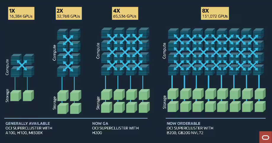
Fuelled by LLMs, the scale of AI computing clusters is growing exponentially. Dell’Oro Group data reveals that LLM parameter sizes have swiftly expanded from billions to hundreds of billions, prompting AI clusters to scale from hundreds to tens of thousands, or even hundreds of thousands of GPUs.
This expansion not only augments computational deployment but also significantly amplifies the demand for high-bandwidth, low-latency interconnects.
As computing power surges, the demand for interconnect bandwidth escalates even more rapidly. Typically, when the number of XPUs (including GPUs and custom AI accelerators) doubles, the corresponding interconnect bandwidth requirement jumps by approximately 2.5 to 3 times.
J.P. Morgan predicts that by 2030, the share of network equipment in data center capital expenditures (CapEx) will increase from the current 5%~10% to 15%~20%, underscoring the strategic significance of interconnect technology in AI infrastructure.
Evolution of Photonics Interconnect Technology: From Pluggable Modules to Co-Packaged Photonics
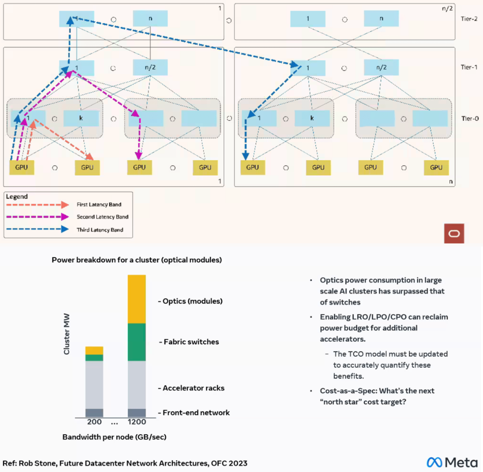
Currently, photonics interconnect technology is widely deployed in scale-out networks in AI clusters, particularly for cross-rack and cross-row connections.
Data centers commonly utilize pluggable optical transceivers to link network interface cards (NICs) and switches, with transmission distances extending up to several tens of meters. However, as LLMs scale, the limitations of traditional optical modules in terms of power consumption and thermal management become increasingly pronounced.
Part 2
Scale-Out and Scale-Up: Technical Evolution of Optical Interconnect Architectures
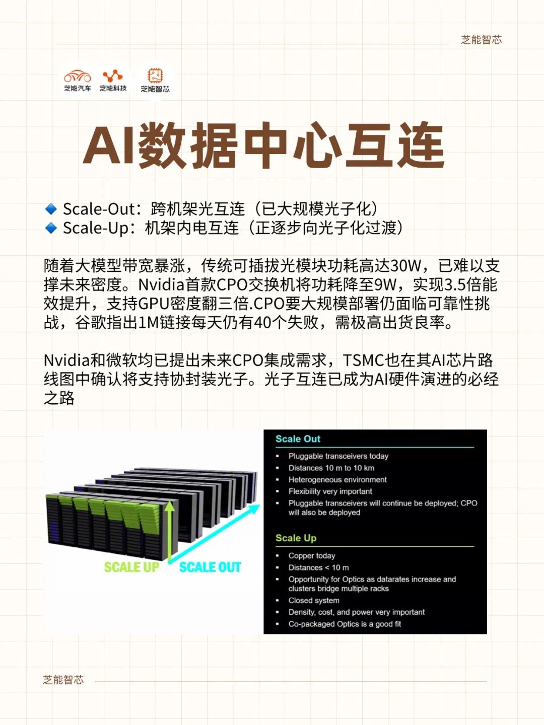
Scale-Out networks have become a成熟 battleground for photonics technology, with optical pluggable transceivers (like QSFP-DD, OSFP) widely adopted for connections between series switches and racks, spanning distances of tens of meters.
Nevertheless, with the gradual commercialization of 400G, 800G, and 1.6T links, power consumption and total cost of ownership (TCO) have emerged as major impediments to their development.
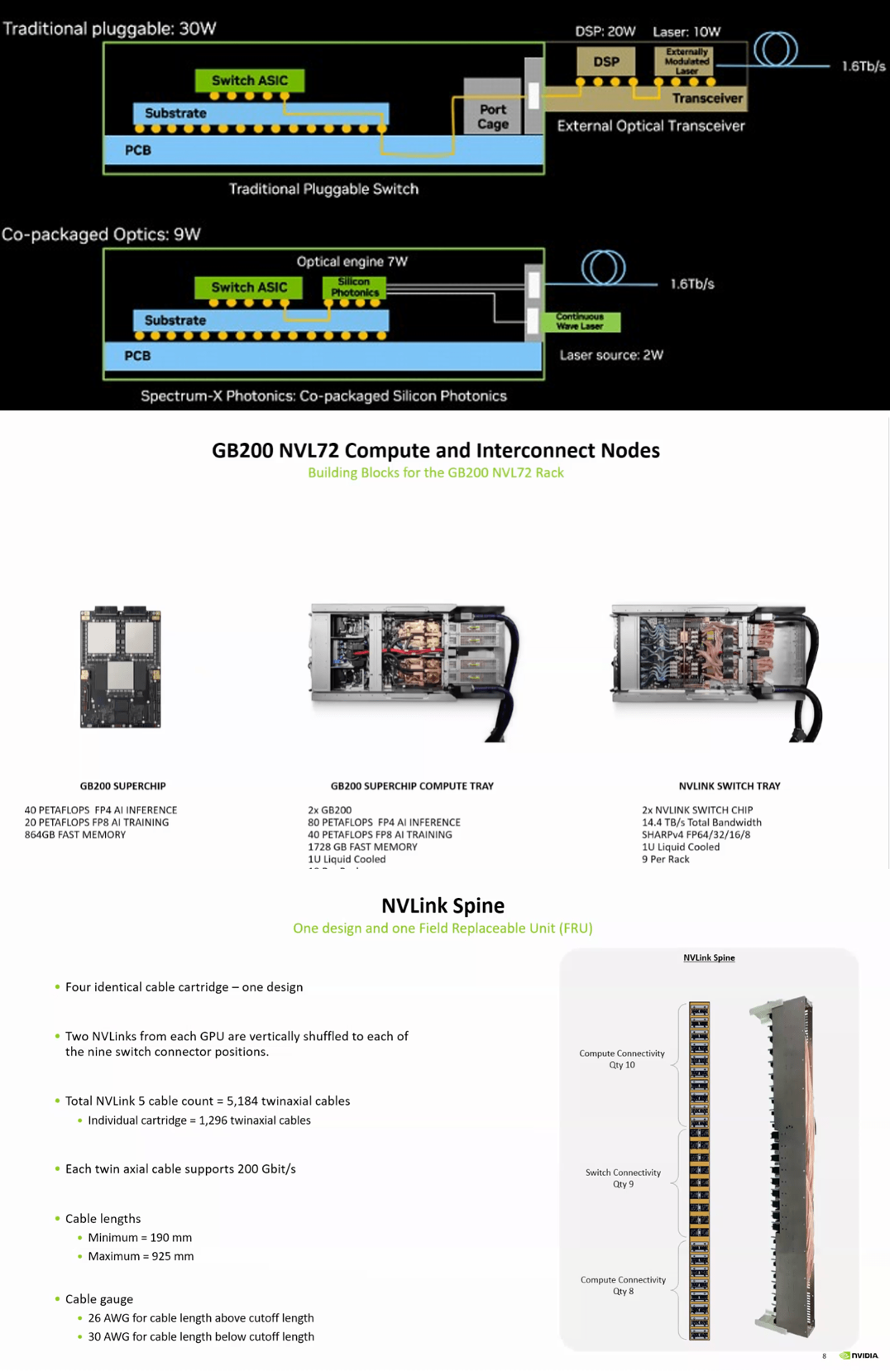
To tackle this, co-packaged optics (CPO) technology emerged and has recently made significant strides. For instance, NVIDIA's Spectrum-X photonic switch, unveiled at GTC25, employs CPO technology, successfully reducing the power consumption of 1.6Tbps links from 30W to 9W, achieving a power savings of approximately 3.5 times.
This reduction not only enhances energy efficiency but also substantially increases GPU density: within the same rack power budget, the number of GPUs can be multiplied by 2 to 3 times.
However, CPO technology still grapples with reliability and yield challenges. Given the massive scale of AI data centers, akin to smartphones, millions of links may experience numerous failures daily. CPO must meet stringent failure rate requirements (e.g., 0.001%/day) and pass large-scale testing to validate its feasibility.
In the realm of Scale-Up networks, copper interconnect currently reigns supreme, with all-copper cables like NVLink72/576 used for intra- and inter-GPU board interconnects, offering high bandwidth while relying on precision PCB and backplane designs to ensure signal integrity.
However, as signal rates approach tens of GHz, limitations such as restricted copper cable length and cable crossing become more evident, posing significant design hurdles.
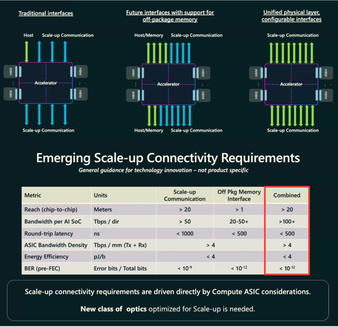
Against this backdrop, CPO technology exhibits immense potential in Scale-Up networks but also encounters numerous obstacles.
Microsoft has underscored the need for a unified physical layer interface for CPO in future AI accelerators, necessitating high bandwidth, low latency, and multi-protocol support within a single package.
NVIDIA, TSMC, and other industry partners are collaborating to develop pertinent CPO standards. This technology is anticipated to be initially deployed in rack-level interconnects within single GPU domains and gradually expanded to intra- and inter-board connections.
Furthermore, foundries are gearing up for the development of CPO. For instance, TSMC has reserved CPO process nodes in its latest technology roadmap to provide semiconductor-level support for future CPO packaging.
It is foreseeable that with the advent of 3nm and more advanced nodes, the integrated packaging of AI chips and photonic modules will become a reality, propelling the entire industry to new heights.
Summary
The swift integration of photonics technology into the AI domain of data centers underscores that the dual-wheel drive of "computing power + interconnect" is reshaping the entire industry chain.
Scale-Out networks achieve significant advancements in power efficiency and density with CPO technology, enabling the realization of ultra-large-scale AI clusters. Meanwhile, Scale-Up networks are evolving towards "copper-to-photonics" to provide foundational support for achieving true human-machine fusion computing.
In the coming decade, with the continued reduction in CPO costs, acceleration of interface standard unification, and gradual resolution of yield and reliability issues, photonic interconnects will transition from being an "optional architecture" to a "standard feature of data center infrastructure." From the cloud to the edge, from within chassis to cross-rack, every connection in data centers will depend on photonics technology, fully unleashing the energy efficiency and scaling potential of AI computing power.
-
On the Eve of Its IPO, Avatr Finds Itself Embroiled in a 'Farce of Controversy and Belittlement'
-
![]()
Yutong Optics' Japanese Subsidiary Unveiled in Tokyo, Shifting Strategic Focus to Technology-Driven Growth
-
![]()
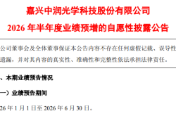
Half-Year Revenue Outstrips Last Year’s Total! Zhongrun Optics Forecasts 80.2% H1 Revenue Growth
-
![]()
Why Does AI Competition Start with Computing Power?
-
![]()
Apple AI Finally Makes Its Debut in China, Yet iPhone's 'AI Autonomy' Faces Uncertainty
-
![]()
Apple AI and QianWen Make Up Lessons: Alibaba Has Its Own 'Doubao Phone'
-
![]()
QianWen Joins Apple, Signal for Large Models to ‘Fade into the Background’
-
![]()
The ‘Anchor’ Strategy of Google Hidden Behind the Bleeding Financial Report