Tesla's New AI Chip Strategy: Transitioning from Dojo to AI5 and AI6 Inference Engines
 08/21 2025
 722
722
On August 7, 2025, Elon Musk announced a pivotal strategic shift, stating that Tesla would streamline its internal AI chip design efforts. This included disbanding the Dojo supercomputing team, as mentioned in our previous article "Breaking News: Tesla Disbands Dojo Supercomputing Team and Business," to focus on inference chips supporting real-time decision-making for autonomous vehicles and robots. 
Musk believes it is inefficient for Tesla to divert resources by simultaneously developing two distinct AI chips—Dojo for supercomputing training and AI 5/6 for inference applications. He envisions Tesla's AI5, AI6, and subsequent chips to excel in inference while maintaining competency in training, thus concentrating all efforts on the AI 5/6 chips.
For training within supercomputer clusters, Musk proposes combining AI5 and AI6 chips to form a "Dojo 3" system.
Musk announced that the next-generation AI5 chip will be produced by the end of 2026 and signed a $16.5 billion AI6 chip procurement agreement with Samsung Electronics in July this year, though a production timeline for AI6 was not provided.
So, why is Tesla making this move? How will its AI chips evolve? What technological path will they take?
This article delves into Tesla's AI chip journey, summarizing the architecture and technology of its next-generation chips based on available information, aiming to provide valuable insights.
Dojo Supercomputer and Tesla's AI Ambitions
Launched in 2021, the Dojo supercomputer embodied Tesla's ambition to harness petabyte-scale data from its global fleet to train full self-driving (FSD) models. Built on proprietary D1 chips, Dojo aimed to achieve exascale floating-point operations per second (FLOPS) to accelerate neural network training.
Analysts praised this project for its scale, valuing Dojo at $500 billion due to its potential to disrupt the data center computing market.
However, by 2025, as discussed in our article "Settled! Model Y is the 'Affordable Tesla': A Deep Dive into Cost Cuts," Tesla's financial reports faced setbacks due to factors like the rise of Chinese electric vehicles. For example, in Q2 2025, Tesla's global deliveries dropped by 14%, sales fell by 12% to $22.4 billion, marking the largest decline in at least a decade. Profits shrank by 16% to $1.1 billion.
These developments highlighted the resource and cost issues surrounding Dojo's development: advanced process nodes for custom silicon require significant capital expenditures and long lead times. Parallel investments in training and inference architectures strained engineering resources.
Moreover, the engineering challenges of scaling from prototype modules to full-size pod architectures were substantial. 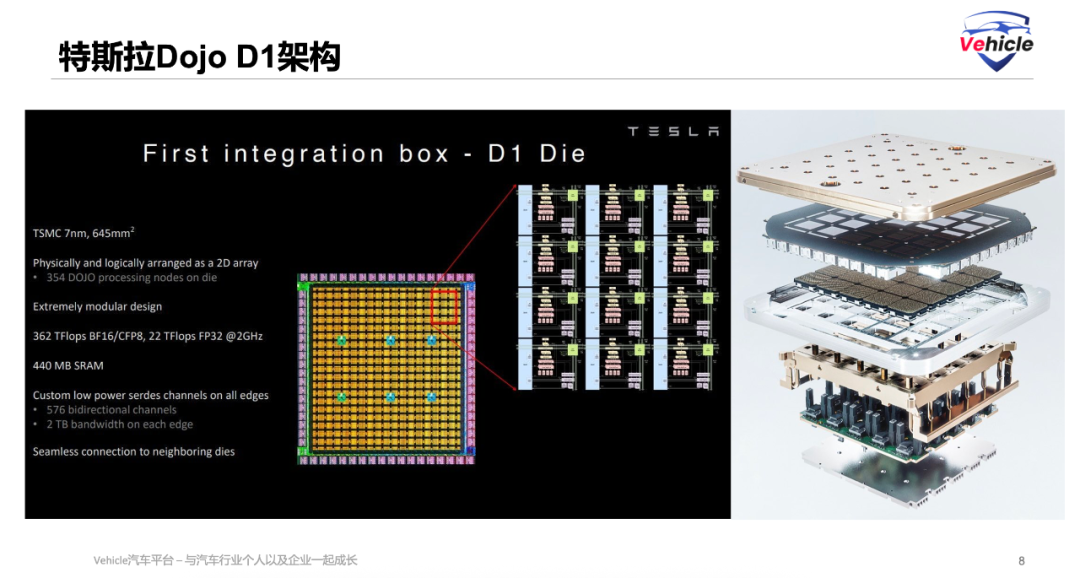
Additionally, the rapid advancements made by AI chip giant NVIDIA posed a significant challenge. 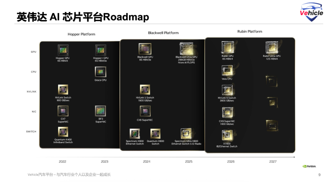
By mid-2025, Tesla internally recognized that maintaining two distinct chip architectures—Dojo for training and AI 5/6 for inference—was not optimal.
However, there are also reports suggesting that Dojo was essentially an experiment for AI6, meaning AI6 might adopt Dojo's technical theories.
Decoding Tesla's AI5 Chip
Tesla's AI5 chip is scheduled for production in 2026. According to online sources, AI5 is expected to reach 2000–2500 TOPS (trillion operations per second) using int8 precision, with a peak power of 800 watts.
Architecturally, AI5 features advanced matrix multiplication engines, supports mixed precision (FP16, BFLOAT16, INT8), and employs a unified cache hierarchy to optimize FSD task performance.
The design of AI5 was completed in July 2025, but due to strategic adjustments and export restrictions, production was delayed to the fourth quarter of 2026.
Given its high performance, AI5 faces export restrictions, requiring performance-limited versions in certain markets to comply with US regulations. A two-tier restriction system limits purchases by "friendly countries" and imposes additional restrictions on "competitive countries," likely leading to a castrated version of AI5 in the Chinese market.
So, what key technologies does Tesla's AI5 adopt?
Heterogeneous Computing Cores: AI5 employs a heterogeneous architecture composed of three cluster types:
- Tensor Accelerators: These fixed-function units handle batch matrix multiplications at 16-bit and 8-bit precision, supporting common AI primitives (convolutions, GEMM, fully connected layers). Utilizing systolic array topology, each tensor accelerator achieves an efficiency of >1TFLOP/W.
- Vector DSPs: Programmable cores optimized for irregular workloads (activation functions, element-wise operations, normalization, indexing). They adopt a VLIW (Very Long Instruction Word) architecture and support predictive execution, reducing pipeline stalls in branch-intensive code.
- Scalar Microcontrollers: Lightweight RISC-V cores dedicated to control plane tasks: task scheduling, I/O management, and power gating coordination. By offloading non-matrix tasks, tensor accelerators and DSPs can maintain peak throughput.
Compared to purely matrix-centric designs, strategically offloading control and irregular processing can increase overall utilization by 15-20%.
One persistent bottleneck in inference is memory bandwidth. In AI5, Tesla employs high-bandwidth memory integration: packaged HBM3 minimizes data transfer latency between DRAM and compute units. AI5 integrates a multi-layered memory hierarchy:
- SRAM Buffers: Each tensor cluster has a total of 2 MB of local storage designed for sub-1ns access. These buffers cache input activations and weight blocks, enabling zero DRAM traffic for short, repetitive computation loops.
- Unified L2 Cache: A 64 MB high-bandwidth cache implemented in eDRAM sits between the clusters and the global DRAM interface. With a total bandwidth of 2 TB/s, the L2 cache serves as a staging area for larger model parameters and feature maps.
- LPDDR5X External DRAM: AI5 supports up to 24 GB, with each pin operating at 8 Gbps. Tesla's custom memory controller dynamically adjusts frequency and timing based on workload intensity, reducing speed (and power consumption) in scenarios like sparse inference or early exit inference.
Sparse Computation Optimization: Hardware support for dynamic sparsity reduces power consumption during inference, similar to NIO's approach when deploying VLA on NVIDIA's Thor U.
AI inference workloads are becoming increasingly tolerant of lower numerical precision. Tesla adopts a mixed-precision strategy in AI5:
- FP8 and INT4/INT2 Units: For vision and perception models, many layers can be executed in 8-bit floating-point (FP8) or even 4-bit integer with no more than a 1% to 2% drop in accuracy. AI5 integrates dedicated FP8 data paths and INT4 multiply-accumulate units, doubling MAC throughput in quantized mode.
- Dynamic Range Calibration: On-chip calibration circuits monitor activation distributions in the initial batch and automatically adjust the zero point and scale factor for INT4 quantization, eliminating manual quantization steps in deployment.
- Mixed-Precision Scheduling: The software stack, built on an improved TensorRT and Tesla's internal optimizer, schedules each layer with optimal precision. Critical normalization or skip connections run in 16 bits, while highly parallelizable convolutional layers run in 4 bits.
Integrating these mixed-precision modes directly into the hardware data path is crucial. Merely supporting quantization in software is insufficient; the chip must seamlessly switch modes to avoid eroding power efficiency—a factor Tesla's AI5 design considers.
About Tesla's AI6
In addition to AI5, Tesla has signed a $16.5 billion agreement with Samsung foundry to co-develop its AI6 chip. These next-generation devices will optimize node scaling to 3 nanometers or lower and integrate enhanced on-chip interconnects to support clustered inference across multiple chips. Tesla engineers anticipate AI6 to offer 2 to 3 times the performance of AI5 in real-world FSD scenarios. 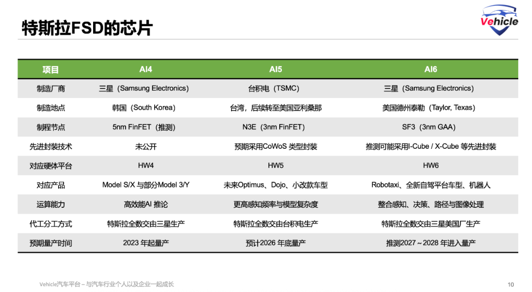
Specific technical information about AI6 is scarce, with some suggesting AI6 is essentially the culmination of Dojo. Therefore, some view Dojo not as a failed project but as an important experimental phase:
- D1 Chip: Large-scale parallel processing validation
- D2 Plan: Precision switch testing
- AI5: Partial validation of a unified architecture
- AI6: Full realization and integration
The progression from configurable deviations to modularity, consistent use of higher-precision intermediate formats, and hardware-level operation interleaving reflect a coherent technical strategy executed by Tesla over the years.
Closing Thoughts
Tesla is a pioneering explorer in physical AI, with successful and cutting-edge software and hardware innovations. However, it is unfortunate that Tesla now conceals its technical information deeply, making it challenging to access the latest relevant technical details. The technical information sources in this article are uncertain, so please consider them carefully. Experts are welcome to leave comments for discussion and exchange.
-
![]()
Can Chinese Automakers Pose Such Fierce Competition? Mercedes-Benz Cancels Year-End Bonuses for 90,000 Staff, Volkswagen to Lay Off 100,000 Employees...
-
![]()
Anhui and Zhejiang Vie for the Crown in New Energy Vehicle Dominance: Who Will Prevail?
-
![]()
Tmall 618 Rankings Unveil Trends Transforming the Home Appliance Industry
-
![]()
This Week in Home Appliances: Overseas Boom! Midea, TCL, Dreame Break Through; Casarte, Fotile, Gree, Hisense, Ronshen Lay Foundations
-
![]()
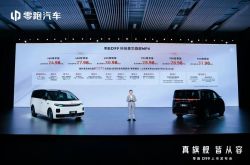
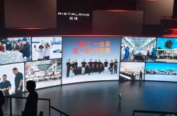
Aiming to Be the Alphard of the Electric Era! After D99's Launch, Leapmotor Will Release All-New Technologies to Pave the Way for a High-End Brand | Mirrormedia Pro
-
![]()
Over 5,200 Orders Placed on First Day: Can the Qijing GT7, Priced from 209,900 Yuan, Compete with the Z7 and SU7? | Mingjing Pro
-
![]()
AI Predicting the World Cup? It’s Time to Stop Insulting AI
-
![]()
iPhone 18 Pro Memory Costs Soar Threefold! Apple Seeks Trump Administration Approval for CXMT Memory Chips