MRAM, the emerging dark horse
![]() 10/14 2024
10/14 2024
![]() 721
721

In 1956, IBM introduced the world's first hard disk drive, RAMAC 305, which could store 5MB of data with a transfer speed of 10K/s. Although this hard disk was enormous, the size of two refrigerators, and weighed over a ton, it marked the beginning of the era of disk storage.
Since then, with technological advancements, memory technology has gradually developed. Dynamic Random Access Memory (DRAM) has faster read and write speeds, meeting the demands of computer systems for rapid data access during operation. Solid-State Drives (SSDs) have gradually replaced traditional hard disks as one of the mainstream storage devices due to their high-speed read and write performance, low power consumption, and shock resistance.
Storage technology continues to evolve, and in recent years, new storage technologies have emerged rapidly, such as Phase Change Memory (PCM), Resistive Random Access Memory (RRAM), Magnetoresistive Random Access Memory (MRAM), and Ferroelectric Random Access Memory (FRAM/Feram).
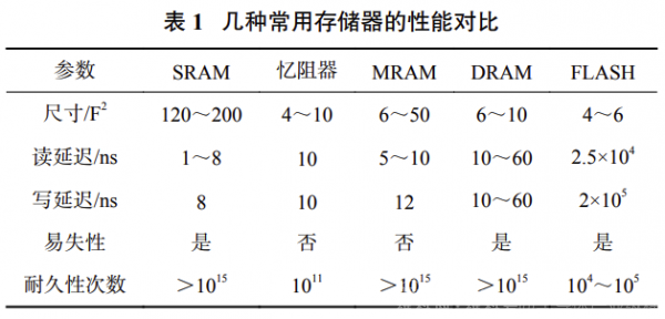
Before introducing MARM, let's briefly understand these four new storage technologies.
Phase Change Memory (PCM) achieves data storage by varying the resistance values through changes in the phase state of phase change materials. A notable example is 3D XPoint technology, jointly developed by Intel and Micron, which Intel branded as Optane and Micron as QuantX.
Magnetoresistive Random Access Memory (MRAM) is based on the Tunneling Magnetoresistance (TMR) effect, featuring unlimited read and write cycles, fast write speeds, low power consumption, and high integration with logic chips. STT-MRAM by US-based Everspin is a representative product.
Resistive Random Access Memory (RRAM/ReRAM) achieves resistance changes by creating or closing conductive channels in resistive materials. Representative companies include Crossbar, Panasonic, and Synopsys Semiconductor.
Ferroelectric Random Access Memory (FRAM/Feram) stores data using the polarization properties of ferroelectric materials, offering fast read and write speeds, low power consumption, and non-volatility. It is applied in embedded systems with high requirements for read and write speeds and power consumption.
Amidst the continuous innovation in storage technology, Magnetoresistive Random Access Memory (MRAM) stands out as a new type of storage technology. Firstly, it combines non-volatility with high-speed read and write capabilities. Compared to traditional non-volatile storage technologies, MRAM's read and write speeds rival that of memory without the risk of data loss upon power loss, a significant advantage in applications requiring fast startup and persistent data storage.
Secondly, MRAM boasts fast read and write speeds. DRAM typically operates at around 50 nanoseconds, while NAND Flash ranges from hundreds of microseconds to several milliseconds. In contrast, MRAM can achieve read and write speeds below 10 nanoseconds. Advanced MRAM products even achieve read speeds of 2-3 nanoseconds and write speeds as low as 2.3 nanoseconds.
Moreover, MRAM consumes low power. Compared to traditional DRAM, MRAM can reduce power consumption by 50%-80% due to DRAM's need for constant refresh operations to maintain data, whereas MRAM's magnetic material-based storage mechanism eliminates the need for frequent refreshes.
Lastly, MRAM integrates well with logic chips, allowing for close integration of storage cells and logic circuits on the same chip, reducing device size, enhancing performance, and lowering costs. This high integration opens new possibilities for the miniaturization and intelligent development of future electronic devices.
The concept of MRAM dates back to the mid-20th century, when scientists began exploring the possibility of using magnetic materials for data storage. With in-depth research into magnetic materials and electronics, the fundamental principles of MRAM gradually emerged.
Early ideas involved representing binary data ('0' and '1') by controlling the magnetization direction of magnetic materials. This storage method offered potential advantages of non-volatility, high speed, and low power consumption, attracting widespread attention in the scientific community.
Early experiments faced numerous challenges, notably the precise control of magnetization direction in magnetic materials. Since magnetization processes are often random, an effective method for directional magnetization was needed. Additionally, early MRAM experiments struggled with low storage density, slow read and write speeds, and poor reliability.
A New Opportunity Brought by Giant Magnetoresistance (GMR)
In 1988, French scientist Albert Fert and German scientist Peter Grünberg independently discovered the Giant Magnetoresistance (GMR) effect, which caused a sensation in the scientific community and significantly advanced MRAM development.
The GMR effect refers to a significant change in resistance in magnetic materials when the magnetic field varies. This effect enables more precise detection of the magnetization state of magnetic materials, improving MRAM's read and write speeds and storage density. Furthermore, GMR provides new technological avenues for MRAM manufacturing, facilitating its integration with traditional semiconductor fabrication processes.
In MRAM technology, the GMR effect is primarily realized through Magnetic Tunnel Junctions (MTJs), a sandwich structure consisting of two magnetic layers and an insulating layer. When the magnetization directions of the two magnetic layers are parallel, resistance is low; when antiparallel, resistance is high. By detecting changes in MTJ resistance, the magnetization state can be read. Meanwhile, applying an external magnetic field or current can alter the magnetization direction, enabling data writing.
Subsequently, the Tunneling Magnetoresistance (TMR) effect emerged, building upon the GMR effect. Compared to GMR, TMR offers higher magnetoresistance ratios and lower power consumption.
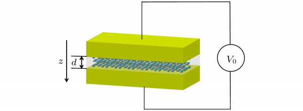
Schematic of MgO-based Magnetic Tunnel Junction Source: Acta Physica Sinica, "Theoretical Study on Temperature-Bias Phase Diagram of MgO-based Magnetic Tunnel Junction"
TMR technology's development can be traced back to the 1990s, when scientists began exploring ways to enhance magnetoresistance ratios using tunneling effects. Significant breakthroughs were achieved in the early 21st century, including the development of MgO-based MTJs with high magnetoresistance ratios and excellent temperature stability, laying the foundation for MRAM's commercialization. Additionally, new manufacturing processes and technologies like self-alignment and perpendicular magnetization were developed to enhance MRAM performance and reliability.
MRAM Enters Commercialization
With the continuous development and maturation of TMR technology, the first commercial MRAM product was launched in 2006 by Freescale Semiconductor (now part of NXP Semiconductors). Manufactured using 180nm CMOS technology, it boasted a 4Mb storage capacity and 35ns read and write speeds, marking MRAM technology's official entry into commercialization.
During this period, MRAM technology continued to improve, enhancing storage capacity, read and write speeds, and operating temperature ranges. Everspin introduced non-volatile Toggle-MRAM with SRAM speeds and flash memory architecture, offering a 16-bit 32MB parallel MRAM with a maximum write cycle time of 35ns and an operating temperature range of -40°C to 125°C, suitable for industrial and automotive applications.
As semiconductor manufacturing processes advanced, MRAM progressed to more advanced technology nodes. For instance, in 2017, Everspin mass-produced 256MB DDR3 STT-MRAM integrated with 40nm CMOS, while in 2019, the company produced 1GB DDR4 STT-MRAM on 28nm CMOS.
Collaboration among major semiconductor manufacturers and research institutions in the industry has intensified, driving MRAM technology's development and commercialization. For instance, Samsung and STMicroelectronics signed a comprehensive multi-sourcing manufacturing agreement for 28nm FD-SOI technology in 2014, supporting MRAM's commercialization.
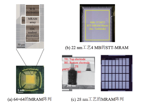
Recent MRAM Chips
Today, the MRAM family encompasses Spin-Transfer Torque (STT), Spin-Orbit Torque (SOT), Voltage-Controlled (VCMA- and VG-SOT), and Domain-Wall MRAM.
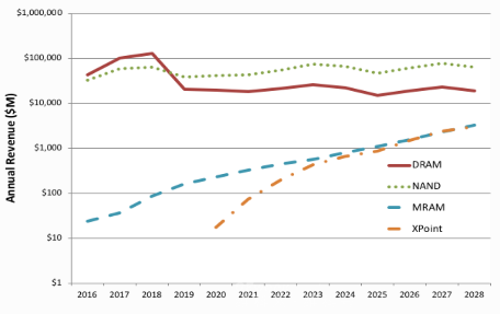
MRAM Market Trends
According to Yole Development, by 2024, the MRAM market is projected to grow 40-fold, with manufacturing processes shrinking to 16nm and storage capacities increasing from 1Gbit to 8Gbit. International semiconductor giants like Intel, Samsung, and TSMC are actively investing in MRAM research and development.
TSMC
In January this year, TSMC announced the successful development of a Spin-Orbit Torque Magnetoresistive Random Access Memory (SOT-MRAM) array chip with Advanced Industrial Science and Technology Research Institute (AIST), marking a significant breakthrough in next-generation MRAM memory technology. This innovative product adopts an advanced computational architecture and consumes just 1% of the power of comparable STT-MRAM technologies. TSMC has successfully developed 22nm, 16/12nm MRAM product lines, securing significant orders in memory and automotive markets.
Samsung
In 2021, Samsung Electronics published the world's first in-memory computing research based on MRAM in the prestigious academic journal Nature. By constructing a new MRAM array structure and running AI algorithms like handwritten digit recognition and face detection on a 28nm CMOS-based MRAM chip, accuracies of 98% and 93% were achieved, respectively.
In December 2022, Samsung Electronics presented a paper titled "World's Most Energy-Efficient MRAM Technology for Non-Volatile RAM Applications" at the prestigious IEEE International Electron Devices Meeting (IEDM), describing nvRAM product technology based on Samsung's 28nm and 14nm logic process nodes.
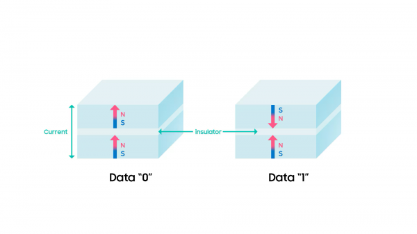
Source: Samsung
Specifically, the enhanced Magnetic Tunnel Junction (MTJ) stacking process technology significantly reduces write error rates (WER). The MTJ has shrunk from a 28nm node to a 14nm FinFET process, reducing its area by 33%. This chip size allows for more chips to be produced on the same wafer, resulting in more die. Additionally, read cycle times have accelerated 2.6 times, and the 16Mb package size has shrunk to an industry-minimum commercial size of 30mm. This solution offers near-infinite endurance with over 1E142 cycles at -25°C. Most importantly, it achieves industry-leading energy efficiency with active read and write power consumption of 14mW and 27mW, respectively, at a bandwidth of 54MB/s.
Intel
Intel announced that its MRAM is ready for mass production, utilizing a mature 22nm FFL FinFET manufacturing process with a yield rate exceeding 99.998%. However, specific details on production scale and target products have not been disclosed.
Intel's MRAM research boasts a cell area of 0.0486 square microns and a capacity of 7MB, with read times of 4 nanoseconds at 0.9V and 8 nanoseconds at 0.8V, write times of 10 microseconds at -40°C, a write endurance of over one million cycles, and a standard operating temperature range of -40°C to 125°C.
Everspin
As an early adopter of MRAM products, Everspin continues to iterate and upgrade its offerings. Following the 2012 launch of its first-generation STT-MRAM (Spin-Transfer Torque Magnetoresistive RAM), the company introduced its second-generation STT-MRAM manufactured using GlobalFoundries' 28nm process, packaged in DDR4, supporting 8-bit or 16-bit interfaces with a transfer rate of 1333MT/s (667MHz) and an increased capacity of 1GB (128MB).
Everspin's MRAM products have penetrated various sectors, including computer memory, aerospace, industrial automation, automotive electronics, and healthcare.
Domestically, numerous universities such as the Chinese Academy of Sciences, Tsinghua University, Fudan University, University of Electronic Science and Technology of China, and Beihang University have achieved notable results in MRAM-related fundamental research.
Beihang University's Spintronics Chip Team within the School of Integrated Circuits has long conducted interdisciplinary research in spintronics. In 2018, the team successfully developed a double-interface MTJ device based on a single-atom layer of tungsten, achieving a Tunneling Magnetoresistance (TMR) ratio of 249%, which remains the world's highest TMR ratio for MRAM chips. The team's proposed double-interface MTJ device structure has become a highly recognized mainstream approach in the industry.
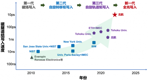
Source: Beihang University
In 2022, the team internationally achieved a new type of magnetic tunnel junction device with a write speed reaching the order of 10 picoseconds (10^-11s) for the first time, surpassing the existing prototype magnetic storage chip technology by 1-2 orders of magnitude in terms of write speed.
The Key Laboratory of Microelectronic Devices and Integrated Technology at the Institute of Microelectronics of the Chinese Academy of Sciences has focused on magnetic storage and spintronic device research since 2019, mainly addressing the key technical issues limiting the development of MRAM from a physical mechanism perspective. For example, in 2023, the institute developed an etching "stop MGO" process based on vertical magnetic anisotropy SOT-MTJ, solving the etching short-circuit problem in SOT-MRAM manufacturing and improving device yield and uniformity of key parameters.
Simultaneously, many emerging memory chip companies in China are increasing their R&D investment in MRAM. Zhidezhen Storage (Beijing) Technology Co., Ltd., founded in 2019, has a research and development team that has been deeply involved in the field of spin memory chips for nearly a decade. It is the only domestic manufacturer with complete intellectual property rights for SOT-MRAM and 8-inch R&D, pilot, and mass production lines. It has successfully developed China's first MRAM core device below 80nm, becoming a leading frontier technology innovation enterprise in the industry. The company has received strategic investments from multiple parties, including ZKStar, Puhua Capital, and CETC Hikvision, and plans to build a new generation of 8-inch and 12-inch memory chip production lines.
Shenzhen Hengcun Technology Co., Ltd., founded in 2019, is currently the only domestic fabless enterprise focused on the design, development, and sales of chip products related to magnetic random-access memory (MRAM) technology. Targeting the intelligent needs of the edge and end sides, it has deployed two core product lines: "standalone MRAM memory chips" and "AISOC chips" containing embedded MRAM.
In 2021, it received an exclusive order for a custom chip, and the customer quickly placed an additional order for a second custom product. As of 2021, the company had a chip integrating over 200MB of MRAM for the first time awaiting sample testing, and two customer-customized chips had been taped out and were scheduled for mass production the following year. Additionally, there were two ongoing research projects based on near-memory and in-memory computing using MRAM.
Zhejiang Chituo Technology Co., Ltd. has made significant progress in the field of MRAM. With Series B funding of 1.2 billion yuan, the raised funds will be used for serialized product development, technological capability enhancement, process platform optimization, market expansion, and industry resource integration, further accelerating R&D and industrialization processes, leading technological innovation in the new storage industry, and improving the MRAM industrial ecosystem layout. The company has a pilot line for 12-inch new storage chips, successfully developing standalone storage chips and embedded IP products, and providing comprehensive services such as chip design, process R&D, tape-out, and test analysis at multiple advanced process nodes including 90/40/28nm.
Conclusion
The emergence of MRAM has injected new vitality into the development of storage technology.
In the future, the integration of MRAM with other storage technologies will be an important development direction. For example, combining MRAM with dynamic random-access memory (DRAM) and flash memory can fully leverage the advantages of various storage technologies to achieve the optimal balance of performance, capacity, and cost. For instance, in mobile devices, MRAM can be used as cache memory in a hybrid storage system with DRAM and flash memory, enhancing device performance and battery life.
Furthermore, MRAM can also be integrated with AI chips to realize a computing-in-memory architecture, improving the operational efficiency of AI algorithms. For instance, in image recognition and speech recognition, AI chips with computing-in-memory can achieve higher performance and lower power consumption.
In today's information age, the importance of storage technology is self-evident. Let us jointly anticipate the outstanding performance of MRAM, this "dark horse," in the storage field.
