Disassembling the iPhone 18 Pro: Apple's 2nm Chip Takes Center Stage, What Chips Are Used in the Supply Chain?
 10/12 2026
 361
361
Produced by Zhineng Zhixin
Consumers look at iPhones for their cameras, battery life, and benchmark scores. The semiconductor industry looks at iPhones to see which chips Apple is using now and what interesting content they offer.
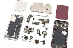
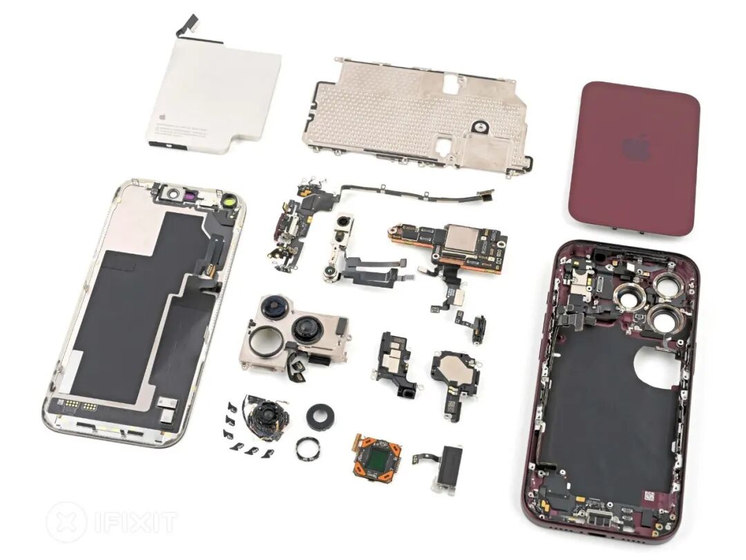
In September 2026, REWA Technology disassembled the iPhone 18 Pro with a physical SIM card, while TechInsights disassembled the U.S. version of the iPhone 18 Pro Max (A3473). Here’s the information to share with everyone.
A20 Pro: 2nm is the Entry Ticket, but Packaging is the Real Star of This Generation
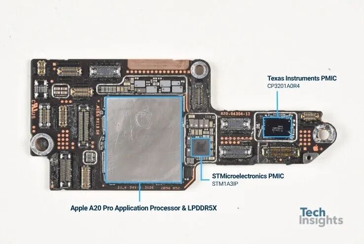
The A20 Pro uses TSMC's N2 process. Compared to the previous generation's FinFET, this node switches to GAA (Gate-All-Around) nanosheet transistors, offering better channel control and reduced leakage.
TechInsights' preliminary measurements show a computing die area of approximately 98.2mm², featuring a hexacore CPU, heptacore GPU, and an increasing proportion of neural network-related circuitry.
The 2nm process generates significant attention. Previously, mobile SoCs commonly used PoP (Package on Package), stacking DRAM on top of the processor.
The A20 Pro changes this approach: the computing die and LPDDR5X are placed side by side. When stacked, heat must pass through the top-layer DRAM to reach the heat dissipation surface. Placing them side by side shortens the thermal conduction path, making it easier to manage chip temperatures. At the same time, the memory interface can be made wider.
TechInsights' preliminary report points to a 96-bit memory interface, though the complete circuitry awaits confirmation through packaging-level research.
Manufacturing, packaging, thermal interface materials, and overall device thermal design must now be co-designed. Any weak link in this chain will diminish the advantages of the process technology.
Thermal Management: Vapor Chambers Evolve from Accessories to Core Processor Design Elements
REWA's disassembly shows that the VC vapor chamber in the iPhone 18 Pro is significantly larger than in previous generations, with Apple reporting an approximately threefold increase in coverage area.
These flat, sealed structures rely on the evaporation, flow, and condensation of an internal working fluid to spread heat from a localized hotspot across a larger area of the device.
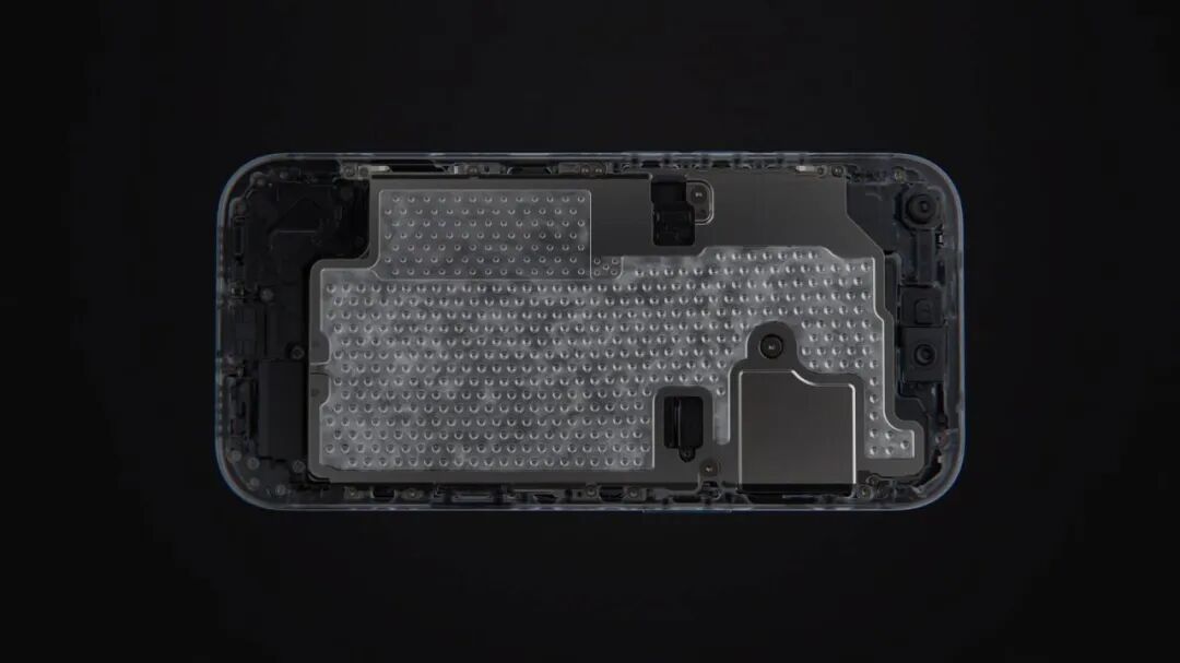
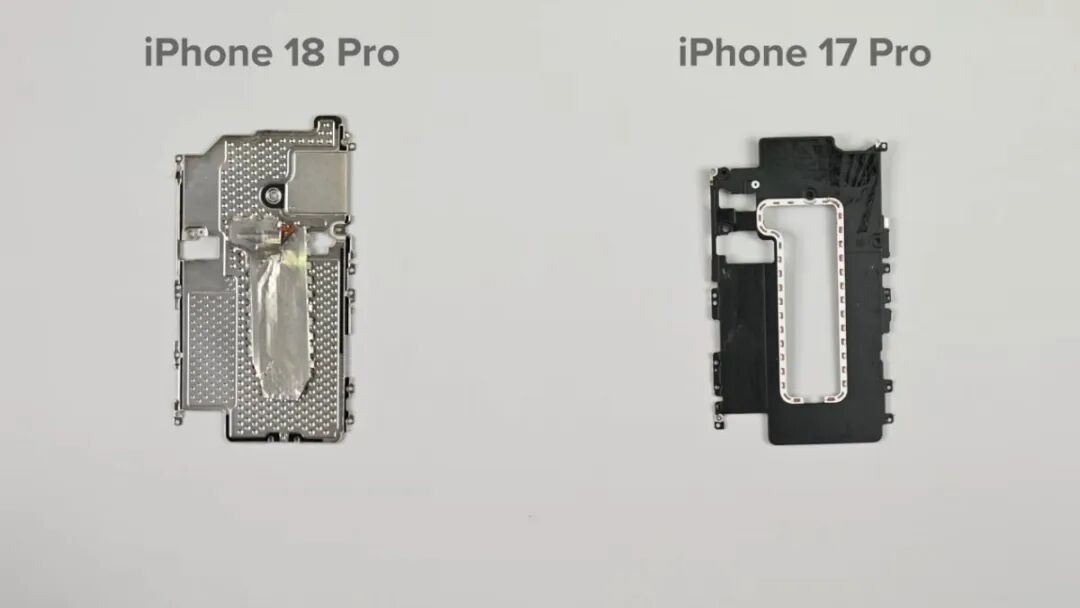
Thermal management ultimately determines sustained performance. It's not difficult for a phone to briefly reach high frequencies; the challenge lies in maintaining temperature and power efficiency during extended gaming sessions, video editing, or running on-device AI models over tens of minutes. VC area, SoC placement, and packaging structure all serve this goal.
Deeper Motherboard Components Make Repairs More Challenging
From REWA's motherboard comparison across generations, the iPhone 18 Pro doesn't simply add one more component. The SoC, interfaces, and shielding structures have all been rearranged, with some NAND storage and power components nestled inside the stacked motherboard.
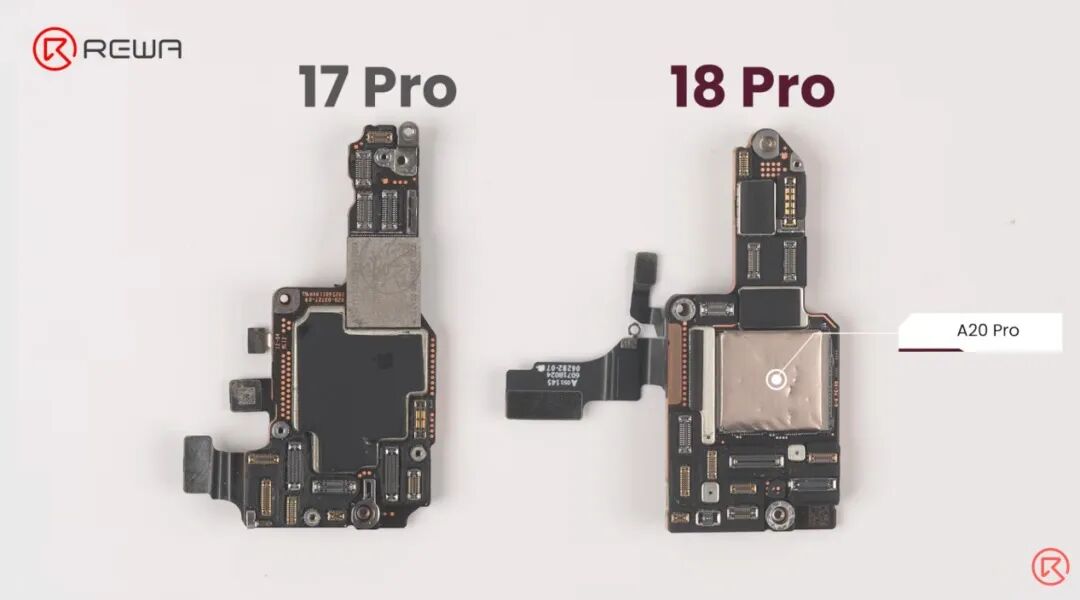
For mass production, 3D stacking improves space utilization, freeing up PCB area for additional components. For board-level repairs, it increases the difficulty of depaneling, desoldering, and reballing. Thus, REWA lists motherboard repairs as one of the most challenging aspects of this disassembly.
Space utilization and repairability have always been a trade-off.
C2 vs. Qualcomm X80: Apple's Custom Baseband Doesn't Eliminate Qualcomm
TechInsights' disassembly of the U.S. Pro Max clearly identifies the SDX80M, Qualcomm's Snapdragon X80 5G baseband, along with the SDR875 RF transceiver. Apple's C2 is installed in the iPhone 18 Pro and Pro Max models sold outside the U.S.
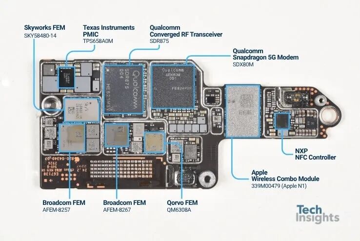
Despite developing its own baseband, Apple hasn't entirely eliminated Qualcomm. Apple hasn't explained why the U.S. Pro Max retains the X80, so it would be presumptuous to attribute it solely to C2's technical immaturity.
Maintaining dual baseband suppliers during a transition period is a common supply chain arrangement. While the baseband handles digital communication and protocol processing, establishing a wireless link requires RF transceivers, power amplifiers, filters, switches, and antenna tuning.
This disassembly also identifies components from Skyworks (SKY58480-14), Broadcom (AFEM-8257/8267), Qorvo (QM6308A), and Qualcomm's QET7100A envelope tracker.
With five RF and analog suppliers represented on a single board, Apple keeps the digital components in-house while entrusting analog and RF functions to specialized manufacturers.
Short-Range Communication: N1, UWB, and NFC
Apple's N1 (module marked 339M00479) manages Wi-Fi, Bluetooth, and Thread connectivity; UWB enables precise ranging and spatial awareness; NFC facilitates close-range identification, secure transactions, and device interactions.
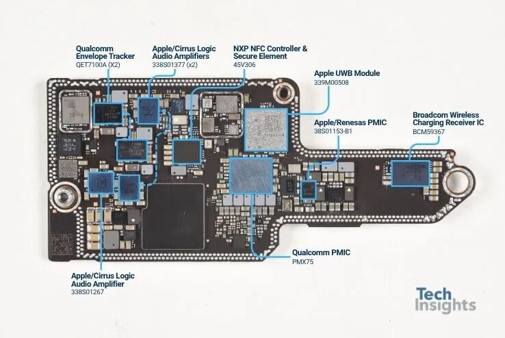
While Apple continues to increase in-house development of core system chips like the A20 Pro, C2, and N1, analog circuits, charging control, power conversion, and security components remain sourced from multiple suppliers.
Camera: Variable Aperture Relies on a Miniature Electromechanical System
The iPhone 18 Pro's main camera upgrades to a variable aperture, using multiple Micro blade (micro-blades) to adjust the light intake. A large aperture suits low-light conditions and shallow depth of field, while a small aperture increases depth of field.
This requires precise alignment between the mechanical structure, driver circuitry, and image processing algorithms.
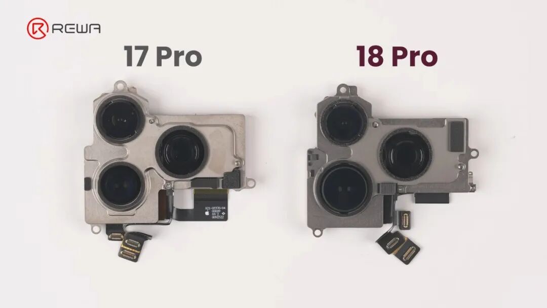
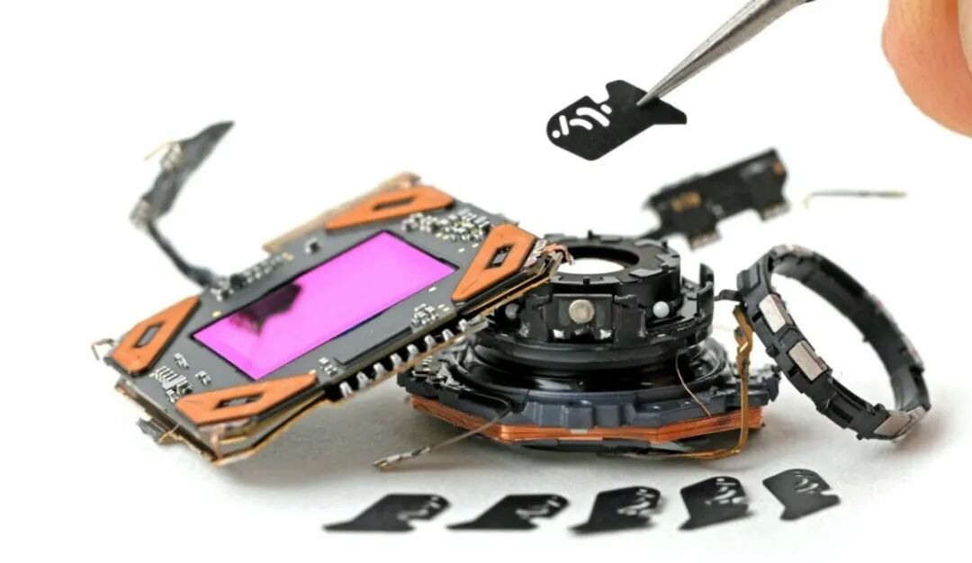
Adding a mechanical action increases component assembly complexity, tolerance control, and repair difficulty. The optical benefits ultimately depend on sensor size, lens specifications, and imaging performance.
Face ID: Dynamic Island Shrinks as Under-Display Optics Become More Precise
The iPhone 18 Pro relocates the Face ID infrared camera beneath the display, with localized OLED pixel array modifications to facilitate infrared light transmission. This reduces the visible size of the Dynamic Island.
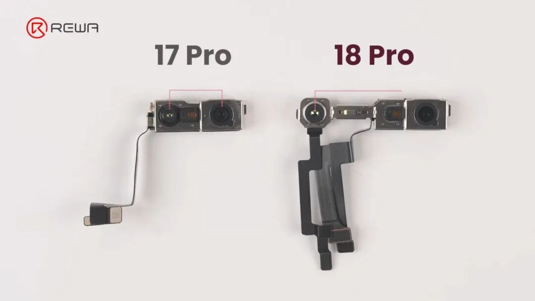
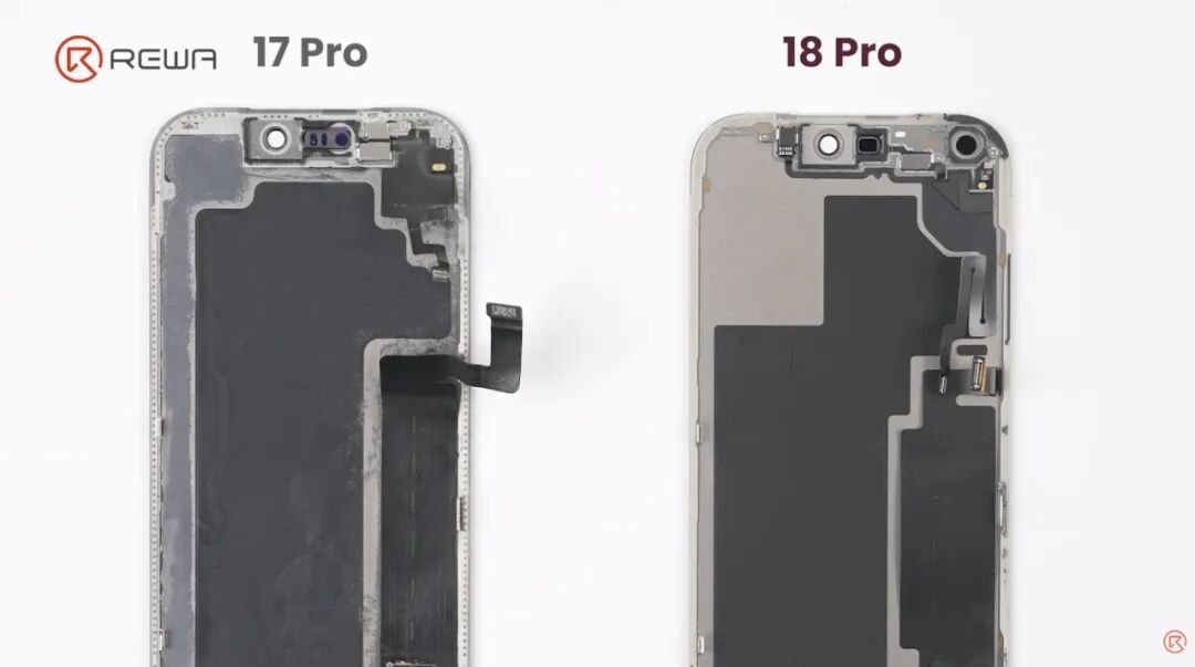
Under-display infrared introduces new constraints.
The screen must simultaneously satisfy display uniformity and infrared imaging quality—two requirements that pull in opposite directions on the same panel. For display suppliers, adding an infrared transmission window increases manufacturing and calibration difficulty.
This under-display implementation applies only to the infrared camera; the front-facing visible light selfie camera hasn't been fully integrated under the display.
Battery and Repairs: Fast Charging Depends on More Than Just the Connector
REWA's disassembly of the physical SIM version reveals a 4,056mAh battery, approximately 1.7% larger than the previous generation's counterpart. The battery connector and some flex cable dimensions have also changed.
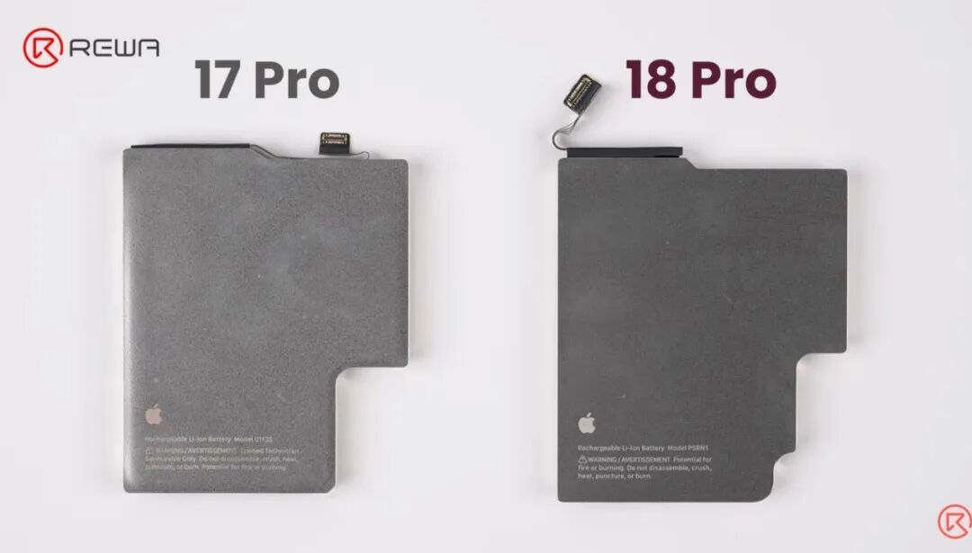
A larger connector improves current carrying capacity and contact reliability, but charging power isn't determined solely by the connector.
The battery cell, PMIC (Power Management Integrated Circuit), temperature control, connector, and charging protocol collectively determine the final charging speed. Disassembly photos can show you that the interface has grown but can't tell you how fast the phone charges.
Summary
What Apple Develops In-House vs. What It Leaves to the Supply Chain
With the A20 Pro, C2, N1, and UWB, Apple continues to strengthen its control over computing and key connectivity chips. Companies like Qualcomm, Broadcom, STMicroelectronics, Texas Instruments, NXP, Cirrus Logic, Skyworks, Qorvo, and Renesas handle RF, power, audio, charging, and interface components.
Apple continues to focus on core computing and baseband development while optimizing thermal management, motherboard stacking, and other engineering constraints.
-
![]()
Disassembling the iPhone 18 Pro: Apple's 2nm Chip Takes Center Stage, What Chips Are Used in the Supply Chain?
-
Stagnant Growth and Unsuccessful High-End Market Entry: Can Li Xueyong Steer Jetour Back on Course?
-
![]()
Is It Possible to Break a Car's Brake Pedal by Stepping on It Too Hard? Can a Driver Fully Depress the Brakes?
-
![]()
Why Aren't More People in the Industry Talking About 360 After Its All in AI Strategy?
-
![]()
Li Auto’s September Insurance Registrations: 31,000 Vehicles, with L6 Outpacing i6 to Secure Top Position
-
![]()
Sub-$150 Entry-Level Smartphones on the Brink of Vanishing: When Will the Storage Shortage Ease?
-
![]()
September Brings Seismic Shifts to China’s Independent Auto Market: SAIC and Leapmotor Join Elite Ranks, Top 5 Expands to Top 7! Three Firms Report Negative Growth Year-to-Date | Mirror Pro
-
![]()
The Era of Lightweight Integration in Existing Assets Arrives! GAC's Entry into FAW-Toyota Holds Multiple Implications