Development Isn't Just 'Washing Away the Exposed Area': How Do Photoresist Sidewalls Take Shape?
 10/16 2026
 543
543

Abstract: Development isn't a straightforward process of "washing away". Positive resists eliminate exposed areas, whereas negative resists remove unexposed regions.
The shape of photoresist sidewalls—whether steep, trapezoidal, or inverted trapezoidal—is influenced by the exposure dose distribution, development selectivity, photoresist type, and thickness. These factors directly affect the accuracy of subsequent etching patterns.
Many have a limited understanding of photolithography development, believing it merely involves "washing away the photoresist in the exposed area."
However, this concept doesn't hold true for negative resists, where exposed areas are preserved rather than removed. The varied forms of photoresist sidewalls are never random outcomes; they are carefully crafted by three key factors: the distribution of exposure depth dose, developer selectivity, and the properties of the photoresist.
Especially in AR waveguide manufacturing, sidewall shape directly influences the fidelity of grating structure formation and is a crucial detail impacting device performance.
I. Development Isn't About 'Washing Away'—It's 'Selective Dissolution'
The essence of development is not merely physical rinsing; it's precise chemical selective dissolution.

The core principle is to leverage the solubility difference of the photoresist before and after exposure to precisely and directionally remove specific areas of the resist layer, achieving patterned formation. Positive Photoresist: In its unexposed state, it resists dissolution by an alkaline developer.
After UV exposure, the photosensitizer undergoes a chemical reaction, producing carboxylic acid substances and significantly increasing solubility. During development, the exposed areas dissolve and are removed, while the unexposed areas remain intact.
Negative Photoresist: The exposed areas undergo cross-linking polymerization, with molecular chains lengthening and molecular weight significantly increasing. The modified resist layer becomes chemically stable and resists dissolution by a developer.
During development, the unexposed areas dissolve and are removed, while the exposed areas cure and are retained. The development logic for positive and negative resists is entirely opposite. The commonly held notion of "development washing away the exposed area" applies only to positive photoresists.
II. How Are Sidewall Morphologies Formed?
The sidewall morphology of photoresists isn't "washed out" by the developer; it's precisely shaped by the exposure gradient differences in the depth direction.
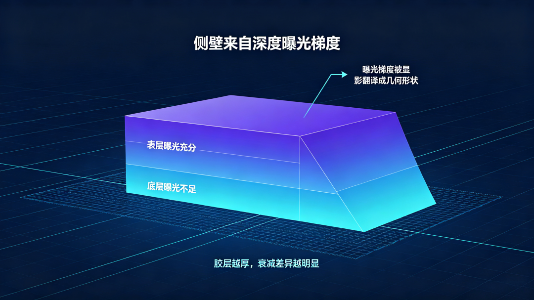
The optical diffraction effects in contact lithography are significant, and the photoresist itself absorbs light. This results in adequate light exposure on the surface layer of the resist and a notable decrease in light exposure at the bottom layer, creating a natural vertical exposure difference.
Taking positive resists as an example: the surface layer is fully exposed and dissolves rapidly, while the bottom layer is underexposed and dissolves slowly. After development, a trapezoidal structure with a wider top and narrower bottom (Over-cut) is formed.
In essence, the sidewall morphology is the vertical gradient distribution of exposure dose, which is transformed into a visual geometric form by the developer. The thicker the photoresist, the more pronounced the exposure attenuation difference and the more evident the trapezoidal distortion effect.
III. Five Key Variables Affecting Sidewall Morphology
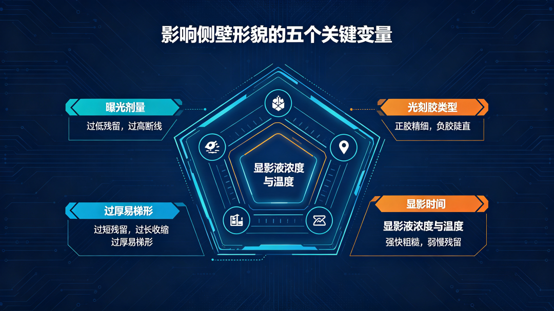
1. Exposure Dose: If the dose is too low, the resist layer is insufficiently exposed, leading to pattern residues and blurry lines; if the dose is too high, the lines are excessively eroded, becoming thinner or even breaking. According to Merck AZ5214E product technical data (TDS) and DTU Nanolab's public process notes: low exposure doses can result in pattern peeling after development; high exposure doses can reduce the depth exposure gradient, and when combined with PEB contrast optimization, nearly vertical ideal sidewalls can be achieved.
2. Photoresist Type: Positive resists are easily soluble in exposed areas, offering high pattern resolution and suitability for fine micro-nano structure processing. However, they have significant drawbacks, such as a tendency to absorb water and swell during development, causing line width drift and affecting dimensional accuracy. Negative resists, after exposure, form a cross-linked dense structure that doesn't absorb water and swell in the developer, resulting in better sidewall verticality. Yet, their overall resolution is slightly lower than that of positive resists.
3. Photoresist Thickness: When the resist layer is too thick, the time required for the developer to penetrate to the bottom significantly increases. The surface layer dissolves completely, while the bottom layer dissolves insufficiently, ultimately curing into a typical trapezoidal shape with a wider top and narrower bottom, disrupting pattern regularity.
4. Development Time: If the development time is too short, a thin resist layer may remain on the top of the pattern, causing blurriness; if the development time is too long, excessive dissolution may occur, causing the line width to shrink and the sidewalls to exhibit tilting or bending defects.
5. Developer Concentration and Temperature: If the developer is too strongly alkaline or the ambient temperature is too high, the dissolution rate becomes too fast, causing the line edges to become rough and burrs to form; if the alkalinity is too weak or the temperature is too low, the dissolution reaction is insufficient, leading to severe resist residue and compromised pattern integrity.
IV. Two Typical Sidewalls: Trapezoidal and Undercut
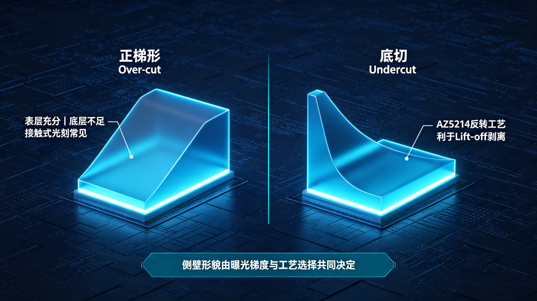
Trapezoidal (wider top, narrower bottom) sidewalls are commonly seen in positive resist processes. When the exposure dose is insufficient or the resist layer is thick, the surface layer is fully exposed while the bottom layer is underexposed. After development, a cross-section with a wider top and narrower bottom is formed, representing the most common sidewall morphology in contact lithography.
Undercut (narrower top, wider bottom, inverted trapezoidal structure) sidewalls are achieved through the AZ5214 exclusive reversal process: a special process of "positive resist → reversal baking → flood exposure → development."
This process allows the surface layer of the photoresist to fully cross-link and cure while the bottom layer remains less cross-linked, ultimately forming a unique undercut sidewall structure. This undercut morphology is a core requirement for the metal lift-off process.
It effectively prevents the deposition of coating materials on the edges and sidewalls of the photoresist, avoiding the formation of a continuous film layer and facilitating the preparation of clean and regular fine micro-nano patterns.
V. What Does This Mean for AR Waveguide Fabrication?
SRG diffractive waveguide masters rely on high-precision electron beam lithography for fabrication.

The steepness of the photoresist sidewalls directly determines the molding fidelity of the grating tooth shapes. Rough sidewalls with burr defects can cause random light scattering in the waveguide modes, exacerbating channel crosstalk and ultimately reducing the imaging clarity of AR devices.
In the mass production of waveguide devices, steep and smooth sidewalls are core process indicators. The reflow process after photoresist patterning can effectively improve sidewall flatness and smoothness, significantly optimizing the device's Q factor and overall optical stability.
The hard bake process can effectively densify the SU-8 photoresist layer, improving sidewall roughness.
Meanwhile, the sidewalls of the photoresist mask may slightly shrink and tilt due to high-temperature baking, a characteristic that precisely meets the process requirements for angled sidewall etching.
Conclusion
The core logic of development isn't simply about "washing away the exposed area"; the dissolution rules for positive and negative resists are entirely opposite.
The unique morphology of photoresist sidewalls is the precise result of the combined effects of exposure dose, development selectivity, resist layer thickness, and process parameters.
In the field of AR waveguide fabrication, sidewall morphology is never an insignificant byproduct of the process. It is a core quality indicator that directly determines the device's optical performance and yield level.
Only by thoroughly understanding the underlying principles of sidewall formation can process parameters be precisely controlled to optimize device performance and production yield.
Interactive Topic: In your photolithography process, do you encounter trapezoidal or undercut (inverted trapezoidal) sidewalls more frequently? Which parameters do you typically adjust to optimize sidewall morphology? Feel free to leave a comment and share your insights.
— AR Andy | Focused on the waveguide and AR micro-display sectors, deeply dissecting the underlying logic of the optical industry
[Risk Disclaimer] This article is for industry popular science purposes only. The technical principles and product parameters are sourced from public technical materials and official information from manufacturers. It is intended solely for industry learning and technical exchange and does not constitute a basis for investment decisions, product selection, or commercial strategies.
-
Big Tech Firms Struggle with Security Concerns in AI Race
-
![]()
Apple AI is Finally Coming to China, But Siri is Not in the First Batch of Features
-
![]()
Unbelievable! TikTok Sellers Lodge Collective Complaint: AI-Generated Sales Videos Distort Product Info, Deceiving Shoppers
-
![]()
New China-EU Automobile Trade Consensus: What Do BMW and Volkswagen's Differing Positions Signal?
-
![]()
Three Departments Launch Investigation into Zunjie; DCD Seals Three Vehicles—Who Will Oversee the Retest?
-
![]()
Development Isn't Just 'Washing Away the Exposed Area': How Do Photoresist Sidewalls Take Shape?
-
![]()
Young Wartime CEO: How to Win Meta's AI Turnaround Battle
-
![]()
7 Million DAU! ByteDance's Free CEO Romance Short Dramas Are Driving Foreigners Wild