SC24 | Google AI Accelerator: TPU v6e Trillium Technology Breakdown
![]() 12/02 2024
12/02 2024
![]() 1800
1800
Produced by Zhineng Zhixin
At the recently concluded SC24 conference, Google officially unveiled its latest TPU v6e Trillium AI Accelerator. This product features comprehensive upgrades in architecture, performance, and data center deployment, marking an important milestone in Google Cloud Services' efforts to meet the demands of Artificial Intelligence (AI).
By enhancing computing power, memory bandwidth, and interconnect performance, the TPU v6e offers improved performance and cost-effectiveness for complex AI workloads such as Transformers, image generation, and convolutional neural networks.
This article will analyze TPU v6e from both chip performance and architectural details, and discuss its future potential.
Part 1
Google TPU v6e: The Secret Behind Its Significant Performance Leap
In the chip industry, balancing performance and cost-effectiveness is crucial for determining product competitiveness.
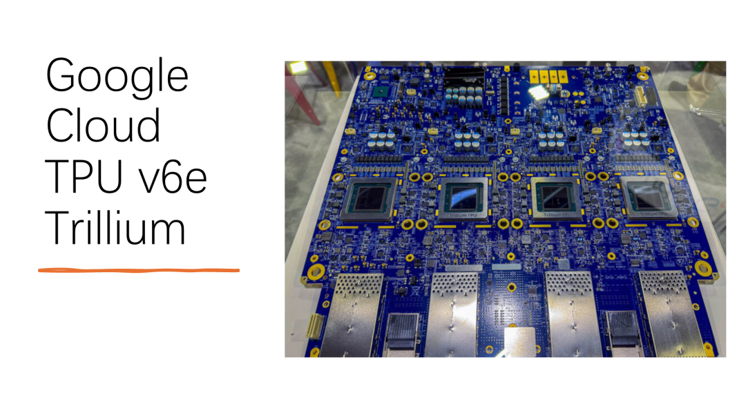
From Google's latest TPU v6e presentation, this generation of products not only surpasses its predecessor, the v5e, in specifications but also achieves higher practical application efficiency through precise system optimization. This is mainly reflected in its leap in performance, memory architecture upgrades, interconnect bandwidth breakthroughs, and dedicated SparseCore support.
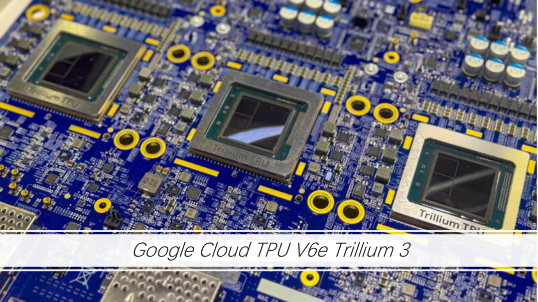
The TPU v6e excels in computing power, with peak computing capabilities for bfloat16 and INT8 formats increased to 918 TFLOPs and 1836 TOPs, respectively, representing a roughly 4.6x improvement over the previous generation. This enhancement is crucial for training and inference of large-scale models, particularly in generative AI and real-time inference applications, where performance bottlenecks are significantly alleviated.
Each chip's High-Bandwidth Memory (HBM) capacity has increased from 16GB to 32GB, and the bandwidth has risen from 819 GBps to 1640 GBps. This not only supports larger model parameters but also significantly reduces data exchange latency, ensuring stability and efficiency in AI training.

The TPU v6e's inter-chip interconnect bandwidth has been increased to 3584 Gbps, with the total bandwidth of a single TPU Pod reaching an astonishing 25.6 Tbps. This high-speed interconnect topology significantly optimizes multi-chip collaboration efficiency, providing a significant advantage for AI models requiring extensive distributed computing.
The introduction of SparseCore is another highlight of the TPU v6e, enabling more efficient processing of sparse matrix operations. This is crucial for sparsity optimization in current AI models, especially in large language model (LLM) training and sparse networks, where performance advantages are evident.
Through these core improvements, the TPU v6e not only outperforms in performance parameters but also provides better unit cost performance. Google claims that despite a slight increase in the price of a single accelerator, its overall total cost of ownership (TCO) is lower than that of the v5e, offering greater value to users.
Part 2
TPU v6e Trillium Chip: Architectural Analysis and Technical Advantages
To fully understand the impressive performance of the TPU v6e, it is essential to analyze its underlying architecture. Here are the key technical details:
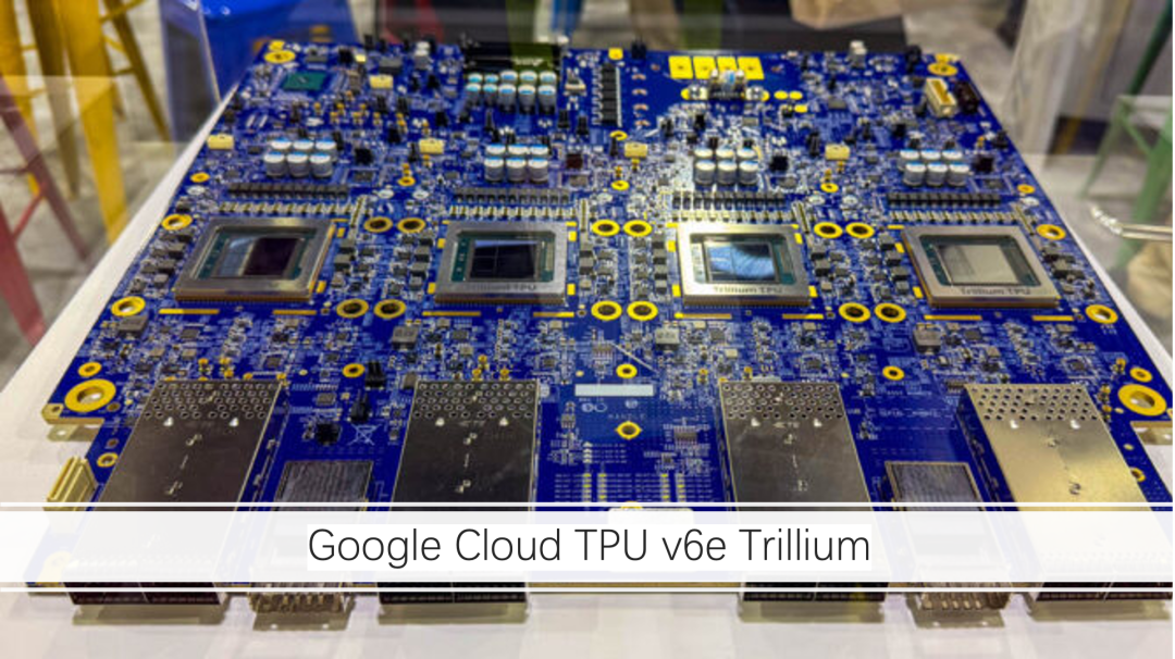
● Each TPU v6e chip contains a TensorCore, which internally comprises four Matrix Multiply Units (MXUs), a Vector Unit, and a Scalar Unit.
This modular design ensures high efficiency in large-scale matrix computations, making it particularly suitable for tasks centered around matrix operations, such as Transformers and CNNs.
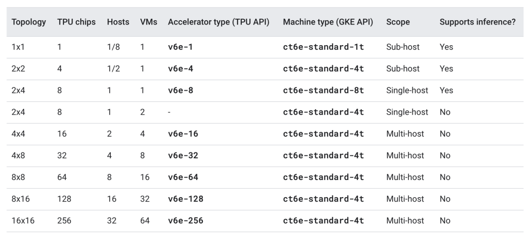
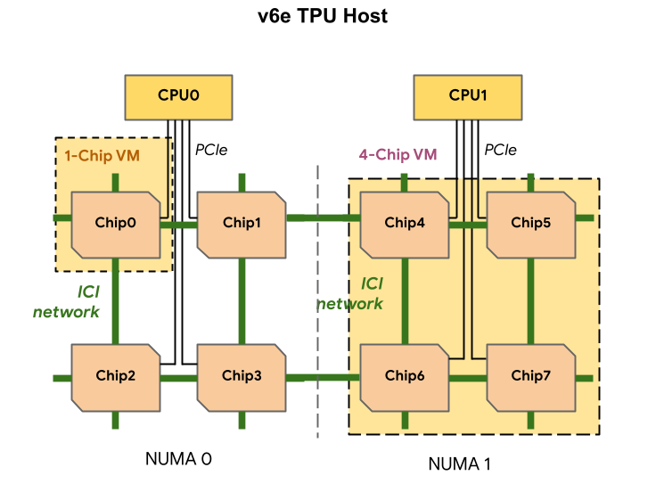
● The TPU v6e employs a 2D Torus topology, with each Pod housing 256 chips. This design significantly increases inter-chip communication bandwidth while upgrading the host network interface from 2 x 100Gbps to 4 x 200Gbps. This not only enhances system throughput but also optimizes scalability for distributed training tasks.
● In terms of DRAM support, each host's capacity has increased from 512 GiB to 1536 GiB, significantly improving support for large-scale training datasets. Especially in inference tasks, the single-host 8-chip (v6e-8) configuration is further optimized, making the entire inference process more efficient.
● The TPU v6e supports various configurations from a single chip to 256 chips, catering to needs ranging from small-scale model testing to large-scale distributed training. In inference scenarios, its 8-chip (v6e-8) standalone mode optimizes latency and resource utilization, providing more flexible options for real-time applications.
The launch of Google Cloud TPU v6e Trillium reaffirms the enormous potential of customized chips in AI computing. From parameter enhancements to system optimizations, this generation of products not only addresses performance bottlenecks but also reduces the overall cost for users, offering significant value to enterprises aiming to rapidly deploy AI capabilities through cloud services.
In the AI accelerator market, Google faces competition from strong rivals like NVIDIA. However, through continuous iteration, Google has maintained its technological leadership. As the trend of in-house chip development gains momentum, with major cloud service providers launching their own accelerators, market competition will further intensify.
Against this backdrop, Google's strategy may focus on further optimizing the balance between performance and cost while promoting the widespread adoption of AI technology.

Conclusion
The success of TPU v6e will hinge on its real-world performance and market acceptance. Given the rising demand for AI computing power, Zhineng Zhixin will continue to monitor this sector closely.
