Who Will Succeed TSMC's Exit from GaN Production?
![]() 07/13 2025
07/13 2025
![]() 798
798

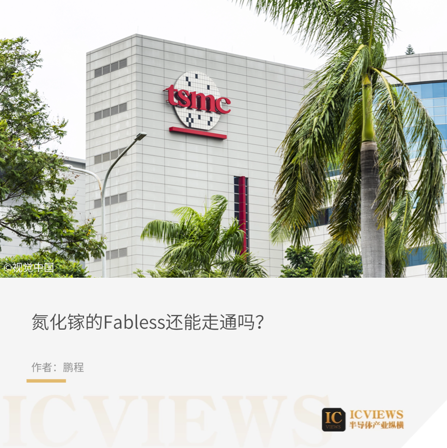
Recently, a cooperation document submitted by Navitas Semiconductor, a prominent global GaN power chip enterprise, has sparked a buzz in the global compound semiconductor industry. The document reveals that TSMC, its long-standing core partner and the world's leading wafer foundry giant, plans to officially cease its GaN wafer production business in July 2027. Concurrently, Navitas Semiconductor announced a partnership with Powerchip Technology to jointly propel the mass production of industry-leading 8-inch silicon-based GaN technology. These developments suggest that the global GaN foundry landscape is poised for a significant transformation.
01
TSMC's Journey with GaN
In the evolution of GaN technology from the laboratory to industrialization, TSMC has been not just a follower but a pivotal driver of the GaN-on-Si technology path, leveraging its profound CMOS manufacturing expertise and forward-thinking vision.
TSMC's GaN strategy dates back to 2011, when GaN power devices were on the cusp of commercialization. Anticipating future energy efficiency upgrades and the surge in high-frequency communication demand, TSMC spearheaded technological research and development. After four years of diligent effort, it successfully achieved mass production of GaN-on-Si technology in 2015, establishing a comprehensive technology platform encompassing multiple voltage levels:
- 650V high-voltage platform: targeting areas with stringent energy efficiency requirements such as power adapters, motor controllers, and PV inverters.
- 100V medium-voltage platform: aimed at server power supplies, notebook power supply systems, and WiFi base station RF power amplifiers (RF-PA) markets.
- 40V low-voltage platform: applied to WiFi and base station RF switches (RF-switch) scenarios.
In the first year of mass production (2015-2016), TSMC attracted over 15 early adopters and completed the tape-out of over 50 new products, laying a robust foundation for business expansion. In 2017, a pivotal turning point arrived with the collaboration with companies like Navitas Semiconductor – TSMC-fabricated Navitas GanFast power ICs began mass shipments, achieving groundbreaking advancements in the fast-charging domain of consumer electronics. By 2023, TSMC had captured 40% of the global GaN wafer foundry market share, forming a "one superpower and two strong players" landscape alongside Germany's X-Fab (33%) and Taiwan's Episil (16%).
Notably, TSMC has emphasized reliability as its core competitiveness since inception. Its GaN products passed rigorous JEDEC certification and even the MIL-STD military standard early on, affirming their stable performance in extreme environments like high temperature, high pressure, and high humidity, paving the way for entry into high-end markets such as industry and communications.
02
TSMC's Strategic Retreat
It's worth noting that previously, Navitas Semiconductor's GaN business was produced by TSMC. However, TSMC has recently been rumored to be exiting the GaN market, with the relevant production lines in its Hsinchu Science Park wafer fabs set to cease operations. On July 3, TSMC issued a statement stating that after a thorough assessment of its long-term business strategy, the company has decided to gradually phase out of the GaN business over the next two years. "We are working closely with our customers to ensure a smooth transition and will continue to meet their needs during this period."
Prior to this announcement, TSMC had demonstrated active involvement and progress in the GaN business. The 2024 annual report revealed that the company's second-generation 650V/100V E-HEMT technology had completed reliability verification and was scheduled for production in 2025. Additionally, TSMC was actively advancing the development of 8-inch GaN-on-Si technology, with production expected to commence in 2026.
TSMC's exit seems somewhat abrupt. The reasons behind this decision are speculated to be the following three points:
- Restructuring of Business Priorities: Siphoning Effect in High-Profit Areas
TSMC's GaN foundry business has a relatively small number of wafer starts, with its current monthly 6-inch wafer capacity being only 3,000-4,000 pieces, with leading customers such as Navitas Semiconductor occupying most of the capacity, contributing minimally to overall revenue. In contrast, the advanced process and packaging business in the AI chip sector exhibits stronger profit attractiveness.
Judging from its current layout, TSMC is shifting its strategic focus, divesting from the relatively low-profit GaN foundry business and turning towards areas with higher demand such as high-performance computing or AI chips. Morgan Stanley data shows that TSMC's CoWoS advanced packaging capacity will increase from 70k at the end of 2025 to 90-95k in 2026, representing a 33% increase. Among them, NVIDIA's Blackwell architecture GPU accounts for 70% of CoWoS-L capacity, with Rubin chips also maintaining incremental growth. Benefiting from the explosion in AI demand, TSMC's advanced packaging revenue share is expected to increase from 8% in 2024 to over 10% in 2025. Shifting the strategic focus towards high-return areas has become an inevitable choice.
- Deterioration of Market Competition: Price Wars Squeezing Profit Margins
Despite the rapid expansion of the GaN market, profitability has failed to meet TSMC's internal expectations. Especially in recent years, new forces represented by Chinese IDM manufacturer Innoscience have leveraged their own 8-inch wafer manufacturing capabilities to form a cost advantage, initiating fierce price competition in the global consumer electronics market. This change is likely to lead the industry into a red ocean scenario of "increasing revenue without increasing profits."
- Raw Material Supply Chain Risks: Gallium Controls Intensifying Cost Uncertainty
On July 3, 2023, China's Ministry of Commerce and General Administration of Customs issued an announcement deciding to implement export controls on gallium and germanium-related items, effective from August 1 of that year. On December 3, 2024, the Ministry of Commerce issued another announcement stating that it would, in principle, not grant licenses for the export of gallium, germanium, antimony, and superhard material-related dual-use items to the United States. These control measures are primarily aimed at safeguarding national security and interests and fulfilling international obligations such as non-proliferation.
Despite some changes in the GaN market this year, such as Wolfspeed, which specializes in third-generation semiconductors like silicon carbide and gallium nitride, announcing bankruptcy reorganization, and TSMC deciding to exit the GaN business, GaN is still regarded as one of the important emerging technologies of the future.
03
The Post-TSMC Era

After TSMC's exit, who will take over?
The industry generally believes that TSMC's silicon-based GaN technology has high compatibility with Powerchip Technology's processes, offering a low-cost transition option for customers like Navitas Semiconductor to switch orders. According to the cooperation plan, Navitas will activate the 8-inch production line at Powerchip Technology's Miaoli Chunan Science Park 8B factory, utilizing 180nm CMOS technology to achieve GaN-on-Si production. This move is expected to form comprehensive advantages in performance, power efficiency, integration, and cost control, with products covering voltage levels from 100V to 650V, precisely meeting the needs of 48V infrastructure (hyperscale AI data centers, electric vehicles).
According to the timeline, the first product certification is expected to be completed in the fourth quarter of 2025, with the 100V series going into production in the first half of 2026, and the 650V products transitioning from TSMC to Powerchip Technology within 12-24 months.
Currently, the mainstream GaN wafer process is primarily GaN-on-Si (gallium nitride epitaxial layer grown on a silicon substrate), mainly concentrated on 6-inch and 8-inch production lines. Taking TSMC as an example, it uses 150mm (6-inch) silicon substrate technology as its core, serving enterprises such as Navitas, STMicroelectronics, and GaN Systems, providing high-voltage GaN wafer manufacturing foundry services. However, due to the overall GaN market size being much smaller than that of CMOS, coupled with pricing that fails to form scale premiums, TSMC's GaN business has consistently maintained a relatively low number of wafer starts.
Now, TSMC has decided to gradually exit the GaN wafer foundry business by 2027. Meanwhile, Infineon is vigorously promoting the self-construction of a 300mm GaN wafer IDM production line, aiming to gain a first-mover advantage in efficiency and cost. The two major players have chosen different paths and strategies.
With the continuous growth in demand for GaN semiconductors, Infineon is capitalizing on this trend to solidify its position as a leading vertically integrated manufacturer (IDM) in the GaN market. Recently, Infineon announced that its scalable GaN production on 300mm wafers is on track. With the first samples to be provided to customers in the fourth quarter of 2025, Infineon is expected to expand its customer base and further consolidate its position as a leading GaN giant.
Infineon's production strategy primarily adopts the IDM model, which encompasses the entire semiconductor production process from design to manufacturing and selling the final product. The company's in-house production strategy is a key differentiator in the market, offering multiple advantages such as higher-quality products, faster time-to-market, and excellent design and development flexibility. Infineon is committed to supporting GaN customers and can expand capacity to meet their demand for reliable GaN power solutions.
Leveraging its technological leadership, Infineon has become the first semiconductor manufacturer to successfully develop 300mm GaN power wafer technology within existing high-volume production infrastructure. Compared to existing 200mm wafers, chip production on 300mm wafers is technically more advanced and significantly more efficient, as the larger wafer diameter enables a 2.3-fold increase in chip production efficiency. These enhanced capabilities, combined with Infineon's strong GaN expert team and the industry's most extensive IP portfolio, are well-suited to meet the rapid proliferation of GaN-based power semiconductors in industrial, automotive, consumer, computing, and communication fields, including AI system power supplies, solar inverters, chargers and adapters, and motor control systems.
It is worth considering that against the backdrop of low profits and limited scale in the GaN foundry market, the survival space for the Fabless model is facing a test. Infineon, with its IDM model combined with the technical and cost efficiency of large-size wafers, may lead the industry into a new competitive dimension.
Despite short-term shocks caused by events such as Wolfspeed's bankruptcy reorganization and TSMC's exit, GaN, as a core technology of third-generation semiconductors, remains recognized as one of the most promising emerging technologies of the next decade due to its irreplaceability in fields such as efficient energy conversion and high-frequency communication. This industry reshuffle triggered by TSMC's exit may accelerate the transformation of the GaN industry from 'technological breakthrough' to 'scale implementation'.


