Revolutionizing Computational Chip Cooling: A Shift Towards System-wide Collaboration!
 07/21 2025
 619
619
Produced by Zhineng Zhixin
With the relentless surge in computational chip power density, thermal management has emerged as a pivotal bottleneck, hindering the advancement of system performance and stability. Evolving from early reliance on two-dimensional heat sinks and fans to today's comprehensive innovations in three-dimensional integration, heterogeneous packaging, AI-driven scheduling, and advanced materials engineering, the frontiers of cooling technology are continually being expanded.
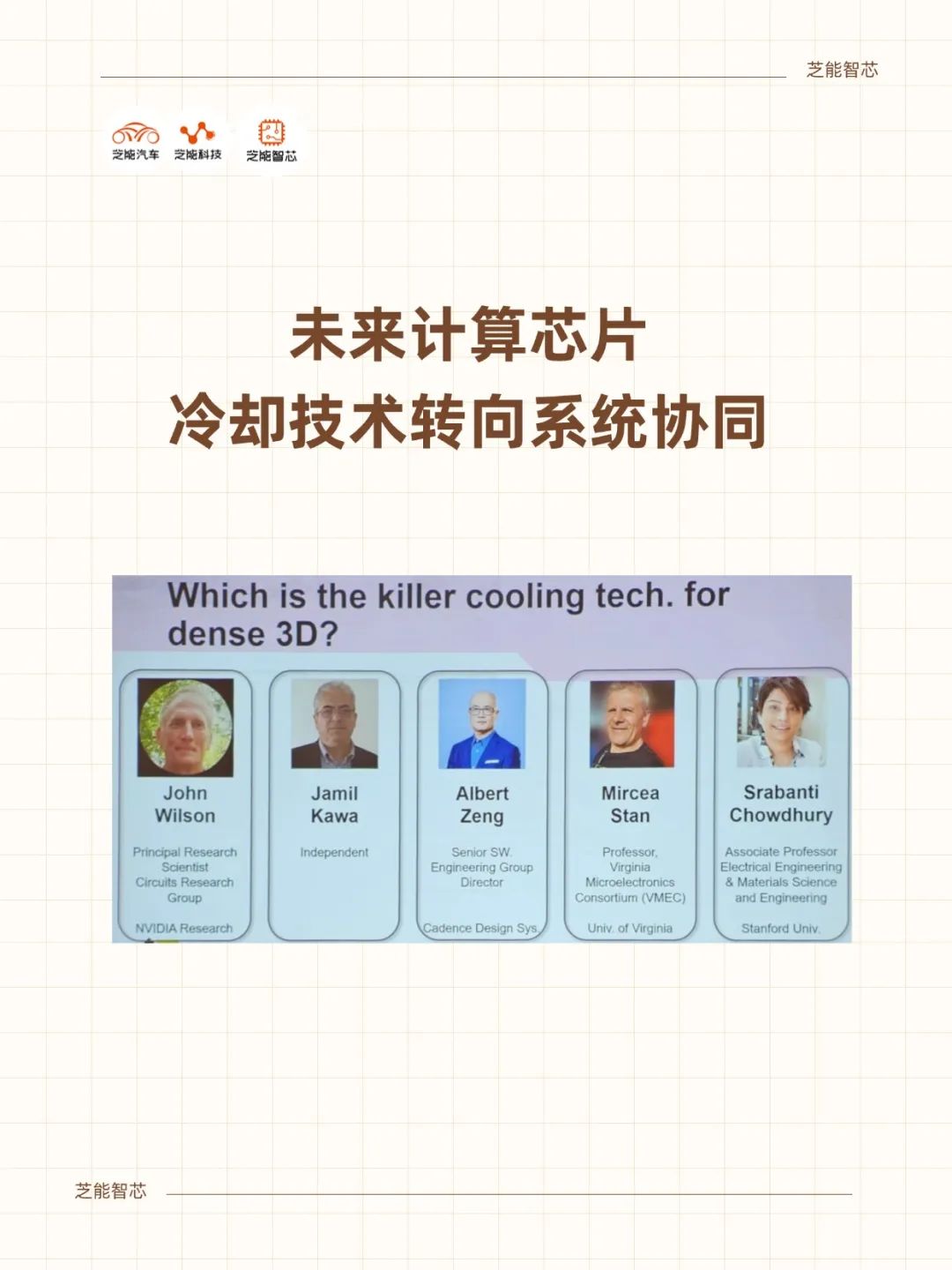
At the 2025 DAC Conference, a panel of experts delved into "Future Cooling Strategies for Computing," showcasing how a collaborative approach encompassing circuit design, system architecture, materials science, and liquid cooling/microfluidics can address thermal challenges at the chip, package, and system levels.
Part 1: Cooling Challenges and Circuit-Level Adaptations to Rising Thermal Density
Over the past decade, workloads such as AI and high-performance computing have pushed chip design towards peak performance, with power density soaring from 50–100 W/cm² in 2010 to 200 W/cm² in 2020, and thermal design power (TDP) of individual chips exceeding 1000 watts.
NVIDIA's transition from Pascal to Blackwell architectures exemplifies this trend, with a 1000-fold increase in single-chip computing power and TDP jumping from 106W to 1200W.
Such high-density power consumption necessitates a shift, where traditional air cooling and heat sinks alone are insufficient. Cooling strategies must be integrated into the design phase, optimized from the device level, layout and routing, placement of thermally sensitive components, and even the configuration of the Power Distribution Network (PDN).
Temperature-aware design has become a cornerstone in the evolution of EDA tools.
◎ Layout and routing tools now incorporate built-in temperature models to avoid clustering high-power modules.
◎ PDN optimization technology uses dynamic current distribution modeling to prevent local hotspots from overheating due to current overload.
◎ In advanced packaging, 2.5D chiplet structures distribute high-heat components across the silicon interposer, with Through-Silicon Vias (TSVs) leading out local cooling paths, becoming a design highlight.
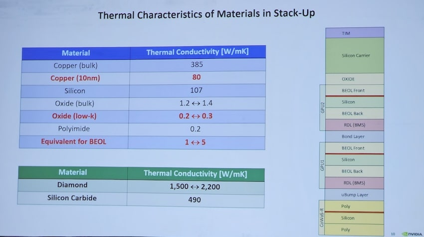
To tackle the vertical thermal barrier in 3D packaging structures, researchers propose incorporating high thermal conductivity materials like diamond and silicon carbide as stacking intermediaries, paired with multi-layer copper heat sinks and laterally laid nano-copper meshes to enhance thermal diffusion and vertical conduction.
While these techniques primarily act at the chip design stage, their core logic shifts from "how to dissipate heat" to "how to design chips that are easier to cool," integrating cooling as a design constraint, gradually transitioning from backend engineering to frontend EDA processes.
Chip thermal design has surpassed 1000W, necessitating the introduction of temperature-aware design tools at the circuit level. Concurrently, chiplet and small-chip structures separate heat sources to balance thermal loads. High thermal conductivity materials like diamond and silicon carbide are used in the thermal channels of vertical packaging structures, with cooling design now integral to EDA system design, requiring collaboration with layout planning and power consumption analysis.
Part 2: System-Level Collaboration, Material Innovation, and Microfluidic Cooling Solutions
Beyond chip-level optimizations, system-level cooling strategies have undergone significant evolution.
NVIDIA's data centers employ a liquid cooling system with the Blackwell GPU, reducing Power Usage Effectiveness (PUE) from the traditional 1.5–2.0 of air cooling to 1.15–1.2, theoretically doubling energy efficiency. This shift involves more than just a change in cooling media; it also encompasses the integration of thermal design, server scheduling, and chip power management.
Large data centers leverage AI models for predictive temperature-based scheduling of task loads, evenly distributing high-heat workloads in time and space dimensions, supplemented by chip power consumption models for dynamic frequency adjustment, forming a thermal-power collaborative scheduling mechanism.
This mechanism, in turn, influences chip architecture design, such as the interleaved layout of memory and computing units, and the cold and hot distribution of heterogeneous cores.
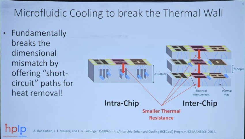
At the material and structural level, the "silicon microchannel cold plate" stands out. This structure introduces nanoscale cooling channels on the chip's backside, allowing coolant to directly contact the heat-generating area, achieving efficient heat exchange.
Research from EPFL demonstrates that in high-heat flux scenarios, microchannel technology offers far superior heat dissipation capabilities compared to air cooling and traditional liquid cooling, making it ideal for temperature-sensitive applications like 3D-IC and quantum computing.
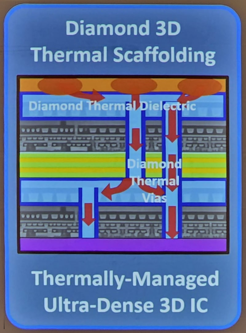
A Stanford University research team has proposed a three-dimensional thermal scaffold using diamond as a thermoelectric medium. The diamond framework below the transistors can quickly dissipate heat on a nanoscale. While still in the laboratory stage, this technology showcases the potential for "horizontal + vertical" bidirectional heat dissipation in future 3D chips.
System-level cooling technology encompasses multiple dimensions, including cooling media selection (e.g., liquid nitrogen-cooled low-temperature CMOS), building design (earthquake-resistant steel damping structures), and voltage stacking, gradually forming a holistic thermal management strategy spanning chips, packaging, to data center infrastructure.
Liquid cooling systems are widely deployed in AI data centers, reducing PUE to 1.15. Microfluidic technology enables direct heat dissipation within chips, suitable for 3D packaging and HPC. Diamond thermal scaffolds present new avenues for nanoscale heat dissipation paths. AI-assisted scheduling drives system and chip design to collaboratively address thermal challenges, while thermal design now extends to building infrastructure levels, balancing seismic resistance and cooling requirements.
Summary
As chip performance improvement is increasingly hindered by thermal constraints rather than logical computing limits, this multi-layered cooling innovation encompassing design, packaging, systems, and materials is paramount. Emerging paths, represented by liquid cooling, microchannels, and diamond materials, transcend single-field technological breakthroughs, fostering a multi-layer collaborative cooling ecosystem.
In this ecosystem, EDA tools, system architectures, scheduling algorithms, and data center designs work in tandem, forming the "thermal management foundation" of the next-generation computing platform.
-
![]()
ByteDance, DJI, and Xiaohongshu Secure Top Three Positions Among China’s Fastest-Growing Unicorns
-
Tesla's in-car voice system in China is finally learning to 'understand human language'
-
![]()
Foreigners Are Amazed: Chinese Electric Vehicle Drive Systems Unveil Innovative 'Poses'
-
![]()
700,000 Brothers and the Future of Robots: Behind JD.com's 'Nirvana Plan'
-
![]()
Zhipu's Trillion-Dollar Valuation: A New Chapter for China's AI
-
![]()
Is Laifen, a 'Dyson Alternative' on the Rise, Now Ensnared by the 'Alternative Curse'?
-
![]()
Beyond Patents: Insta360 and DJI Compete in Retail
-
![]()
Piercing Through Industry Chaos: The Curtain Rises on Compliance for Autonomous Driving