Huawei Releases Latest Chip Packaging Patent: Can Improve Chip Bonding Yield
![]() 11/18 2024
11/18 2024
![]() 523
523
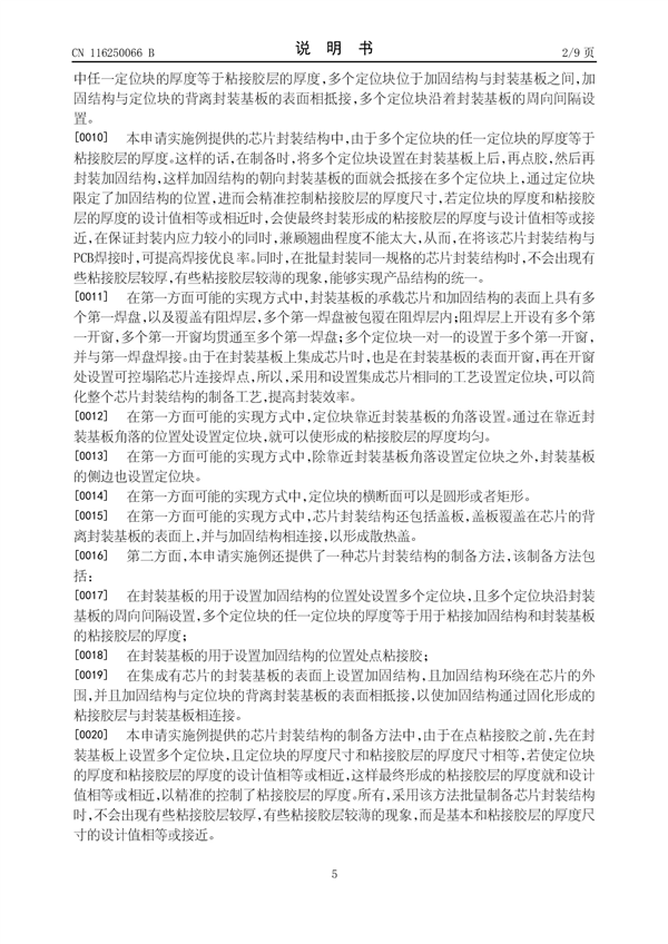
According to Fast Technology on November 17, a search on the official website of the National Intellectual Property Administration today revealed that Huawei Technologies Co., Ltd. recently announced a patent named "Chip Packaging Structure, Electronic Device, and Method for Preparing Chip Packaging Structure" with the authorization announcement number CN116250066B, filed in October 2020.
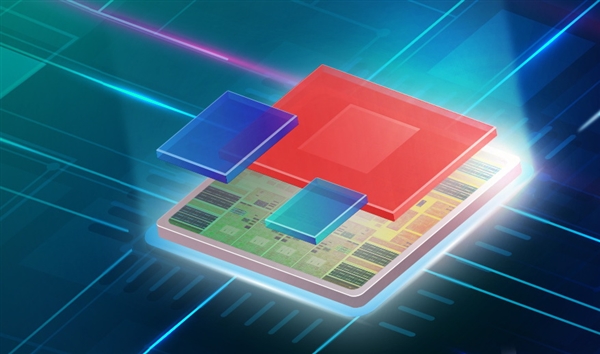
The patent relates to the field of chip packaging technology. The application embodiment provides a chip packaging structure, an electronic device, and a method for preparing the chip packaging structure, primarily aimed at providing a chip packaging structure capable of precisely controlling the thickness of the adhesive layer.
It is reported that due to the surging demand for computing power in high-speed data communication and artificial intelligence, chip integration has further increased. While chip sizes have grown, multi-chip packaging technology has also been widely adopted, resulting in the continuous enlargement of the overall chip packaging structure.
As the size of the chip packaging structure increases, the mismatch in thermal expansion coefficients between the chip and the packaging substrate makes controlling thermal deformation of the package increasingly difficult. Greater thermal deformation can directly lead to significant warping of the entire chip packaging structure.

It is understood that in the chip packaging structure provided by Huawei's application embodiment, since the thickness of any positioning block among multiple positioning blocks is equal to the thickness of the adhesive layer, after placing multiple positioning blocks on the packaging substrate during preparation, glue is applied, followed by packaging reinforcement. The surface of the reinforcement structure facing the packaging substrate will then abut against multiple positioning blocks.

The positioning blocks define the position of the reinforcement structure, thereby precisely controlling the thickness of the adhesive layer. When the designed thickness values of the positioning blocks and the adhesive layer are equal or similar, the final thickness of the adhesive layer after packaging will be equal or close to the design value.
While ensuring low internal stress within the package, the degree of warping must not be excessive, so that when bonding this chip packaging structure to a PCB, the bonding yield can be improved.
Simultaneously, when batch packaging chip packaging structures of the same specification, there will be no inconsistency in the thickness of the adhesive layer, ensuring a uniform product structure.


