After Joining NVIDIA’s Core Supply Chain, This Optical Company Secures Fresh Funding!
 05/13 2026
 672
672
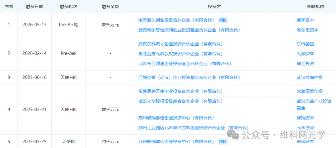
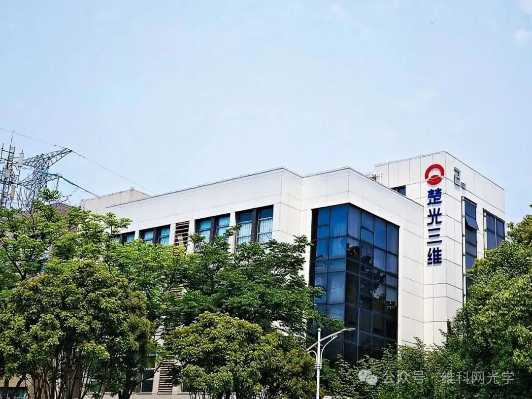
Recently, Hubei Chuguang 3D Sensing Technology Co., Ltd. (hereinafter referred to as "Chuguang 3D") announced the successful completion of its Pre-A++ round of financing, raising tens of millions of RMB. The investor for this round is Xianghe Capital. Since its inception in 2022, the company has consistently attracted investments from leading institutions, including Frees Fund, Oriza Holdings, Optics Valley Venture Capital, and Jiangcheng Technology Innovation Fund.
Why has this optical sensing company, established just over three years ago, been repeatedly favored by the capital market? What are its background and strengths?
Chuguang 3D has ventured into a highly challenging and cutting-edge field: micro-nano optical 3D imaging and metrology inspection. In simpler terms, this involves conducting nanoscale 3D CT scans on semiconductor chips and high-end electronic components.
This sector has long been dominated by overseas giants. Imported equipment is not only prohibitively expensive, with individual units costing several million RMB, but also features closed, non-open-source underlying code. This makes it difficult to adapt to the rapid iteration and flexible production needs of domestic production lines. Chuguang 3D has identified a breakthrough by adopting an entirely new technical approach: area-array confocal 3D microscopic imaging.
Its technical principle is rooted in wide-field microscopic imaging, utilizing structured light illumination to modulate microscopic information on the surface of the measured object. Combined with vertical axial scanning, it captures nanoscale-precision 3D topography in a single snapshot. Unlike traditional laser scanning confocal technology, Chuguang 3D has not followed the conventional path of stacking expensive precision optical hardware. Instead, it has taken a different route by deeply integrating AI algorithms into the 3D point cloud processing workflow. This approach significantly reduces system cost and complexity while maintaining leading technical performance.
This solution offers high compatibility, supporting both a high-precision mode of up to 1 nanometer and a sub-micron precision mode with a large measurement range of 30 millimeters. It can also handle inspection scenarios that were previously challenging to unify, such as smooth surfaces, complex topographies, metal/non-metal heterogeneous surfaces, and even transparent materials.
Based on this technical system, the company has launched two core product lines: the "Area-Array Confocal 3D Microscopic Sensor/Microscope" and the "Line Spectral Confocal 3D Sensor." Both product lines have secured bulk orders and achieved stable delivery.
The success of a hard-tech company ultimately hinges on its team. Chuguang 3D's Chief Scientist, Professor Liu Xiaojun, is the Director of the Department of Instrument Science and Technology at Huazhong University of Science and Technology. With over two decades of deep engagement in micro-nano 3D measurement, he has led the completion of multiple national key projects and accumulated extensive expertise in underlying optical sensing and metrology technologies.
Founder and CEO Li Min completed his undergraduate studies at the School of Optical and Electronic Information at Huazhong University of Science and Technology. After graduation, he co-founded and led startups in the semiconductor and 3D vision sectors, gaining firsthand experience in technology commercialization and market adoption. In 2022, Li Min returned to Wuhan Optics Valley and co-founded Chuguang 3D with Professor Liu Xiaojun, enabling the coupling of cutting-edge laboratory technologies with industrialization thinking.
Developing self-reliant technology is one thing; securing a foothold in the demanding industrial arena is another. In 2024, Li Min's team connected with NVIDIA's core suppliers through alumni networks. Initially, they faced skepticism: Could domestic equipment truly achieve nanoscale precision? Without further ado, the team dedicated themselves to on-site production line testing for over a year.
The results they delivered prompted a reevaluation of this Chinese company: its precision matched that of imported equipment, but its inspection efficiency underwent a qualitative transformation. A process that previously took two hours was compressed to just one minute, representing a two-order-of-magnitude leap in efficiency.
Subsequently, the product smoothly entered NVIDIA's core supply chain and secured tier-one supplier orders from international industry giants. The equipment has been exported to markets such as Vietnam and South Korea, playing a sustained role in safeguarding yield improvement in high-end chip production lines.
Meanwhile, the company has established a nationwide business network covering key micro-nano manufacturing sectors, including semiconductors, new energy, advanced displays, AI computing PCBs, and new materials. It has set up branches and offices in Wuhan, Suzhou, and Shenzhen.
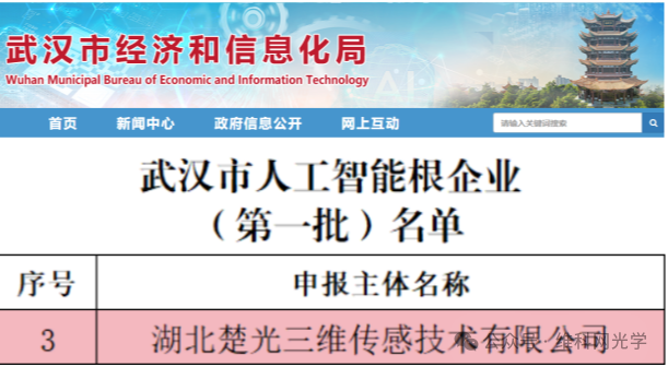
Recently, Chuguang 3D has maintained a high-frequency acceleration in its developments. In March 2026, the company was successfully selected as one of Wuhan's first 20 "AI Root Enterprises," a title aimed at identifying benchmark companies with source innovation capabilities, ecological leadership, and long-term growth potential.
In the same month, it participated as a key project in the centralized signing of Optics Valley optoelectronic information projects, covering key industrial chain segments such as chips, devices, modules, and complete systems.
From technological breakthroughs to capital support, from entering global top-tier supply chains to deeply integrating into local industrial ecosystems, every step taken by Chuguang 3D has aligned with the critical junctures of breaking monopolies and moving toward global competition for domestically produced high-end optical inspection equipment. Breaking monopolies is just the starting point; the future holds great promise.
-
AI's Richest Person Revealed: A Native of Zhanjiang!
-
No one dares to bet big on Seres' financial report
-
Standing at a Distance, Behind Xiaomi's Phone Slowdown and Layoffs", "Xiaomi Phone, Declining Sales, Offline Stores, Product Strategy, Comprehensive Ecosystem of People, Vehicles, and Homes", "Accordi
-
![]()
ByteDance Enters Physical AI, Igniting the Second Wave of 'Feast'?
-
![]()
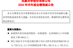
Phoenix Optics Forecasts a Nearly 70% Drop in First-Half Net Profit, Yet Optical Business Profit Shows Growth!
-
![]()
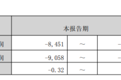
A Staggering 50.16% Reduction in Losses Projected! COST's Interim Report Signals a Pivotal Moment
-
![]()
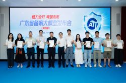
Nearly 19% of National Total! Guangdong Boasts 164 Registered Large Models as New AI Personification Regulations Take Effect
-
![]()
BYD’s Baosha, Sought After by Australians, Makes a Triumphant Return to China