Stress Analysis in Heterogeneous 3D-IC Design: Ensuring Structural Reliability
 06/05 2025
 758
758
Produced by Zhineng Zhixin
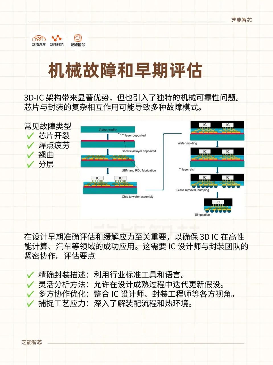
Heterogeneous 3D-IC design has emerged as a pivotal pathway for the relentless advancement of chip performance and integration density. However, it also introduces unprecedented mechanical stress challenges. Issues such as chip cracking, solder joint fatigue, warping, and delamination test the comprehension and control of thermo-mechanical physics by design engineers.
This article delves into stress challenges in heterogeneous 3D-ICs, explores the technical journey from modeling to collaborative design and simulation verification, and anticipates how EDA tools can further bolster the collaborative optimization of packaging and chips, ensuring the implementation of highly reliable advanced packaging.
Part 1
Stress as an Obstacle in the Era of Heterogeneous 3D-ICs
With advanced packaging technology progressing into the 3D IC era, centered around stacking and heterogeneous integration, the physical boundaries between packaging and chips are increasingly blurred, leading to unprecedentedly complex mechanical interactions.
In traditional 2D chip design, mechanical stress from thermal expansion and contraction has a limited impact. However, in a 3D architecture, the disparities in thermal and physical properties among chiplets, interconnect structures, and even interposers can generate significant thermal mismatch stress.
This stress not only results in visible structural damage, such as chip cracking, solder joint fatigue, package warping, and interface delamination, but also subtly alters the electrical characteristics of devices on a finer scale, impacting the functional stability of the overall system.
For instance, high-precision sensors or components that leverage the piezoelectric effect may experience performance drift or even deviate directly from design specifications when subjected to stress disturbances. This is unacceptable in fields like medical equipment, automotive electronics, and infrastructure sensing systems. Additionally, even if core logic circuits do not utilize stress as an input signal source, residual stress can still influence critical path timing or power consumption through factors like mobility changes, leakage current shifts, or interconnect impedance fluctuations.
Thus, 3D IC design is no longer solely an electrical optimization problem but a multiphysics challenge requiring interdisciplinary collaboration.
The intricate interplay of thermal, mechanical, and electrical factors necessitates the design team to conduct comprehensive, multi-dimensional coupled simulation and modeling early in the design process. Otherwise, unpredictability in later packaging stages could translate into a risk of failure.
Part 2
Technical Path from Modeling to Verification
The first step in effective stress management in heterogeneous 3D packaging is to create a high-precision package description model.
This encompasses not only millimeter-scale substrate structures but also nanoscale chip features, particularly in key areas such as high-density interconnects, through-silicon vias (TSVs), and microbumps.
Using standard modeling languages like 3Dblox, different teams can establish semantic interfaces for a unified package structure, laying the groundwork for subsequent thermodynamic simulations.
In the early modeling stages, parameter uncertainty is common, such as when specific packaging material parameters are not finalized and interconnect structure dimensions are still under discussion. However, this does not hinder the use of approximate material models or "black box" assumptions to construct stress estimation scenarios for preliminary sensitivity analysis.
This modular, progressive approach aids in identifying high-risk areas before the design is finalized, providing quantitative guidance for structural layout, thermal management strategies, and even packaging path selection.
It's crucial to note that this is not a solitary effort by IC designers but a systematic engineering project that necessitates collaboration between chip, packaging, material, and simulation teams.
Different stakeholders may have distinct focuses: IC designers are more concerned with the impact of stress on electrical performance, while packaging teams prioritize overall structural strength and manufacturing feasibility.
An effective process involves articulating these concerns within a common model and continuously iterating using finite element analysis (FEA) tools to eventually converge on a design solution that balances structural safety and electrical performance.
The sources of packaging stress extend beyond static thermal distribution, permeating the entire manufacturing process. For example, each process from chip mounting, reflow soldering, to molding, wire bonding, and cooling leaves a stress "fingerprint." Some of these residual stresses can be released with thermal cycles, while others persist permanently, becoming "time bombs" that could trigger cracks or deformations under operational conditions in the future.
The design team must simulate the entire assembly process and capture the stress evolution at each stage through multi-step sequential simulations. This requires tools capable of simulating nonlinear materials and handling boundary transitions for multi-stage process conditions.
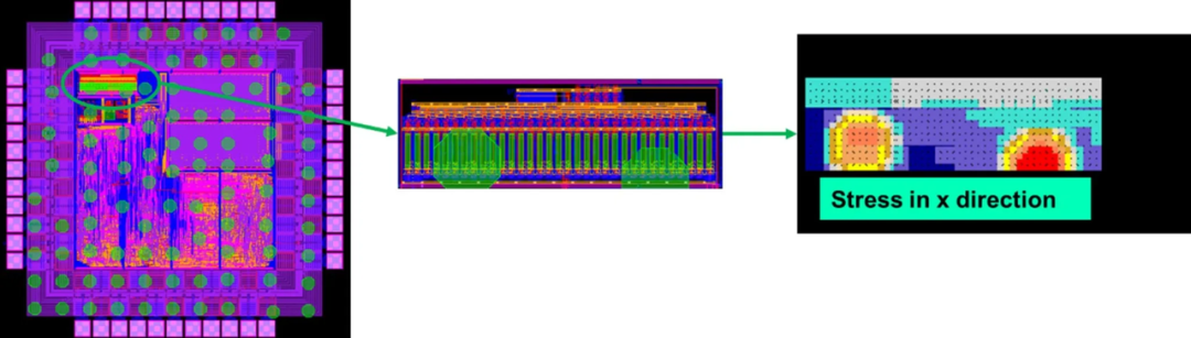
As the design nears completion, the focus of stress analysis shifts to key interface areas, particularly chip-package connection points, TSV areas, and thermally sensitive devices. Through localized refinement simulations, it's possible to assess stress concentration, thereby determining whether the device needs to be migrated or locally reinforced.
Furthermore, considering the relationship between stress and electrical performance is paramount. For example, whether a metal interconnect path exhibits impedance changes under high shear stress and whether this affects signal integrity.
In the final acceptance stage, a comprehensive "stress-performance" closed-loop analysis system is essential. At this juncture, simulation results are not merely a reference for design adjustments but become a critical basis for design sign-off.
Engineers must ensure that the chip can manage the thermo-mechanical coupling effect within the circuit tolerance range under all operating conditions. Coupled with visualization tools, it's possible to intuitively display the spatial distribution of stress on the chip, aiding in the identification of potential hazards and achieving "visual acceptance."
Summary
The complexity of 3D IC stress management stems fundamentally from the sophistication of advanced packaging's physical characteristics and the heightened interconnectivity between design levels. In the past, engineering teams relied more on internally developed simulation scripts or limited standard tools for partial analysis, which is insufficient for the current demands of heterogeneous integration and system-level collaboration.
Fortunately, with the continuous evolution of the EDA tool chain, an increasing number of commercial tools with thermo-mechanical simulation capabilities that can be deeply integrated with chip circuit design data are emerging. These tools support multi-physics collaborative simulation, cross-level model integration, and visual risk assessment, thereby significantly enhancing simulation efficiency and verification accuracy.
-
![]()
ByteDance, DJI, and Xiaohongshu Secure Top Three Positions Among China’s Fastest-Growing Unicorns
-
Tesla's in-car voice system in China is finally learning to 'understand human language'
-
![]()
Foreigners Are Amazed: Chinese Electric Vehicle Drive Systems Unveil Innovative 'Poses'
-
![]()
700,000 Brothers and the Future of Robots: Behind JD.com's 'Nirvana Plan'
-
![]()
Zhipu's Trillion-Dollar Valuation: A New Chapter for China's AI
-
![]()
Is Laifen, a 'Dyson Alternative' on the Rise, Now Ensnared by the 'Alternative Curse'?
-
![]()
Beyond Patents: Insta360 and DJI Compete in Retail
-
![]()
Piercing Through Industry Chaos: The Curtain Rises on Compliance for Autonomous Driving