In-Depth | The Era of High Numerical Aperture EUV Lithography Machines Driven by AI Chips Approaches
 03/05 2026
 565
565
Why the AI Chip Arms Race Has Placed High-NA EUV on a Pedestal
AI computing power has become the sole core driver for advanced-process lithography machines.
Industry data for 2025 shows that AI chip manufacturers' procurement of 3nm and below process equipment has surged by over 30% year-on-year, accounting for more than 30% of total global demand for advanced equipment.
TSMC's allocation of advanced production capacity further illustrates the issue, with over 90% of its 3nm and below process capacity locked in by AI chip firms like NVIDIA, AMD, and Google, while consumer electronics giants like Apple and Qualcomm can only compete for the remaining less than 10% share.
Research by OpenAI reveals that the computing power required for large model training grows tenfold every 18 months, far outpacing the pace of Moore's Law [which states that the number of transistors doubles every 18 months].
To support this exponential growth in computing power, the only path is to integrate more transistors onto a chip per unit area while significantly reducing power consumption and improving energy efficiency.
When chip processes reach 2nm and below, traditional 0.33NA EUV lithography machines have hit their physical limits.
Previously commercialized 0.33NA EUV lithography machines have a single-exposure resolution limit of about 13nm. To achieve processes below 2nm, multi-patterning processes must be used.
However, multi-patterning means an exponential increase in process steps, which not only significantly drives up manufacturing costs but also leads to a sharp drop in chip yield, making it impossible to meet the demand for large-scale mass production of AI chips.
High-NA EUV is the only solution to this pain point. NVIDIA's next-generation B100 GPU, Intel's 14A process AI accelerator, and TSMC's 2nm process AI chip orders—all core players in the AI industry are betting their next-generation products' success on high-NA EUV lithography machines.
This AI computing power arms race has ultimately placed high-numerical-aperture EUV lithography machines on a pedestal, making them the most core strategic asset in the AI era.
500,000 Wafer Verification: Lithography Technology Reaches a Cross-Generational Milestone
Core data disclosed by ASML CTO Marco Posth at the San Jose Technology Conference confirms the mass production readiness of High-NA EUV.
As of February 2026, the equipment has cumulatively processed 500,000 300mm silicon wafers, with downtime kept at extremely low levels, and chip circuit patterning precision fully meeting industrial-scale mass production requirements.
Current equipment uptime has stabilized at 80%, with ASML planning to raise this metric to 90% by the end of 2026.
The processing practice of 500,000 wafers means that ASML has resolved the full range of technical challenges for High-NA equipment, from optical systems to mechanical control, from photoresist adaptation to defect control.
According to the Rayleigh lithography resolution formula, with the EUV light source wavelength fixed at 13.5nm and the process factor k1 approaching the physical limit of 0.25, increasing the numerical aperture (NA) is the only path to break through the resolution bottleneck.
ASML has raised the equipment's numerical aperture from 0.33 to 0.55, a 67% increase, directly elevating the theoretical resolution of the lithography system from the 13nm level to 8nm, successfully achieving single-print imaging of 16nm pitch line/space patterns, setting a world record in lithography technology.
More critically, this leap in resolution was not achieved by sacrificing efficiency or increasing process complexity; instead, it fundamentally simplifies the manufacturing process for advanced chips.
Previously, using 0.33NA EUV equipment to manufacture chips at nodes below 2nm required 3-4 multi-patterning processes for critical metal layers with line spacings ≤20nm, completing patterning through multiple masks in steps.
This not only significantly increased manufacturing time and production costs but also raised chip defect rates, reduced production yields, and even led to higher carbon emissions.
With a price tag of $400 million per unit, double that of the first-generation EUV lithography machine, this figure is enough to make any chip manufacturer weigh their investment decision carefully.
However, behind the seemingly exorbitant price lies a more complex cost-benefit calculation.
According to data disclosed by IBM researchers at the 2025 SPIE Advanced Lithography and Patterning Conference, the cost of a single high-numerical-aperture exposure is about 2.5 times that of a standard low-numerical-aperture exposure.
This price may seem high, but the true advantage emerges when high-numerical-aperture technology replaces complex multi-patterning processes.
For processes requiring three or more low-numerical-aperture masks, switching to single-exposure high-numerical-aperture imaging begins to pay off.
In fact, for four-mask self-aligned lithography etching processes, high-numerical-aperture technology can reduce total wafer costs by about 1.7 to 2.1 times compared to low-mask multi-patterning.
Fewer exposures mean simpler process flows, which can shorten cycle times and reduce the likelihood of overlay errors.
From a long-term return on investment perspective, a single high-numerical-aperture EUV lithography machine has an annual production capacity of about 150,000 wafers. Combined with the high added value of 2nm chips, the annual output value of chips can exceed $10 billion.
The Semiconductor Money Printer of the AI Era: ASML's Monopoly Logic and Market Judgment
The commercial essence of high-numerical-aperture EUV lithography machines is the [admission ticket] to advanced processes.
At process nodes of 2nm and below, without high-NA EUV lithography machines, there is no possibility of mass production.
This irreplaceable scarcity gives ASML absolute monopoly pricing power.
From ASML's 2025 financial report data, annual net sales reached €32.7 billion, with net profit of €9.6 billion and a gross margin stabilized at a high 52.8%.
Among this, EUV lithography machine business sales reached €11.6 billion for the year, a 39% year-on-year increase, with an average unit price exceeding €240 million and a gross margin exceeding 70%.
The gross margin for High-NA EUV is even more astonishing, exceeding 80%, with a per-unit profit exceeding €280 million.
More frighteningly, ASML's orders for high-NA EUV have been booked until 2030. In the fourth quarter of 2025, ASML's quarterly new orders reached €13.2 billion, with a backlog of unfulfilled orders totaling €38.8 billion, of which over 60% were orders for EUV and high-NA EUV equipment.
TSMC, Samsung, and Intel, vying for high-NA EUV production capacity, have even gone so far as to pay full upfront payments to lock in delivery shares for the coming years.
This monopoly-derived commercial value also extends to the full lifecycle service segment.
ASML offers 5-10 year long-term service agreements for high-NA EUV equipment, including equipment maintenance, upgrades, and consumables supply, with annual service fees reaching 10%-15% of the equipment's selling price.
In 2025, ASML's installed base management business revenue reached €8.2 billion, a 26% year-on-year increase, becoming the second-largest revenue pillar after equipment sales.
ASML judges that over the next three years, DRAM manufacturers' procurement of EUV equipment will double, becoming the second-largest demand source for high-NA EUV.
Based on this judgment, ASML has formulated an extremely aggressive technology iteration roadmap.
Even as high-NA EUV has just achieved mass production, ASML has already initiated research and development of 0.75NA Hyper-NA EUV lithography machines, aiming to achieve mass production at processes below 0.5nm in the early 2030s, continuously widening the technological gap with competitors.
In ASML's plan, high-NA EUV will enter a large-scale delivery phase from 2026-2030, becoming the core engine for the company's revenue growth, while Hyper-NA EUV will lock in the advanced process market for the next 15 years.
China's Sineva: Market Layout and the Path to Differentiated Competition
While ASML stands atop the global semiconductor industry with high-NA EUV and EUV lithography machines are strictly embargoed, Shenzhen Sineva Semiconductor's market layout offers a brand-new answer.
Contrary to widespread market perceptions, Sineva has never been a company focused solely on lithography machines. Its core positioning is as a supplier covering the entire front-end semiconductor manufacturing process, building a [group army] of domestic semiconductor equipment.
Sineva has completed layouts in six core technological areas, constructing a product matrix covering key segments such as etching, thin film deposition, metrology and inspection, EDA software, and high-end testing instruments.
Therefore, Sineva's core logic is to achieve self-sufficiency in semiconductor equipment through a full-chain layout, building a closed-loop ecosystem for domestic semiconductor manufacturing.
By covering the entire process of etching, deposition, and metrology equipment, Sineva can provide wafer fabs with complete line process solutions, an advantage that single-equipment manufacturers cannot achieve.
Using dry DUV lithography machines + SAQP process innovation to achieve equivalent 5nm process manufacturing capabilities, precisely matching the core needs of domestic AI chips.
Through the SAQP self-aligned quadruple imaging process, this equipment can achieve equivalent 5nm process capabilities, fully meeting the mass production needs of most domestic AI chips, automotive-grade chips, and IoT chips.
The core advantage of this route lies in its perfect alignment with the current state of the domestic semiconductor industry.
On the one hand, the technological barriers for EUV lithography machines are extremely high, and domestic mass production is not achievable in the short term, while DUV lithography machine technology is relatively mature, with core components easier to localize.
On the other hand, domestic AI chip design companies have already formed a design trend of [de-EUV-ization], and Sineva's technological route precisely matches the needs of domestic chip design companies.
Currently, Sineva's SAQP process has completed validation on SMIC's 28nm production line, achieving an 85% yield. Lithography machine equipment is planned for official mass production in 2026, with a target annual production capacity of dozens of units.
At the same time, Sineva has formed deep ties with Huawei and SMIC, jointly defining technical standards and developing process solutions, forming a closed-loop domestic ecosystem of [equipment-process-chips].
The High-NA EUV Game: Essentially a Struggle for Technological Sovereignty in the AI Era
Future chip performance improvements will not necessarily rely solely on process shrinkage; architectural innovations, packaging innovations, and material innovations could all break the absolute dependence on high-NA EUV.
From Shanghai Micro Electronics' mass production of DUV lithography machines to Sineva's full-chain equipment layout, from the Changchun Institute of Optics, Fine Mechanics and Physics' breakthrough in EUV optical systems to Keyi Hongyuan's research and development of lithography light sources, China's semiconductor industry is steadily breaking through blockades and addressing shortcomings at its own pace.
Partial sources referenced: Semiconductor Industry Observer: "The Next-Generation EUV Lithography Machine Is Coming," Jiguo.com: "$400 Million Per Unit! ASML's New-Generation Lithography Machine Is Ready for Mass Production, AI Chips See Core Breakthrough," MGClouds: "ASML's Next-Generation EUV Set for Large-Scale Mass Production, Chip Industry Landscape to Change," Luoluo's Diary: "The Arrival of High-NA EUV: Lithography Precision Enters the 0.5nm Era?" Mufeng Machinery: "ASML [Slams the Accelerator] on EUV Lithography Machines, Chip Capacity to Surge 50% by 2030"
-
![]()
Smartphone Prices Surge Amid Manufacturer Anxiety
-
![]()
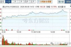
Orbbec Soars to Record Heights, Eyes Further Capital Influx of 980 Million!
-
![]()
Tongding Interconnect Sets Up Shop in Shaoguan with 800 Million Yuan in Registered Capital
-
![]()
Before Kimi’s A-Share Debut, Zhipu Aims to Secure More 'Strategic Funding'
-
![]()
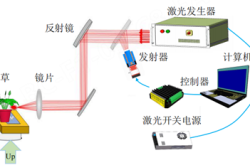
Innovative Leap | Fiber-Pluggable 1470nm Laser Source: Revolutionizing Precision Laser Weeding
-
![]()
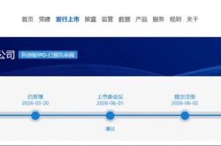
73-Day Rapid Listing: Where Does Unitree's Wang Xingxing's 'Sense of Urgency' Come From?
-
![]()
AI Project Mindverse, Backed by Meituan, Faces Data Inflation Allegations Over Its Macaron Product
-
![]()
3000-word In-Depth Analysis | What Makes Physical AI So Magnetic? It Has Captivated Masayoshi Son, Jensen Huang, and Justin Sun All at Once