MicroLED Hops on the Express Train of Optical Communication
 03/19 2026
 682
682
In just half a year, MicroLED has completed a remarkable track crossover.
Half a year ago, when talking about MicroLED, it was still a highly anticipated new display solution in consumer electronics terminals such as AI glasses. Today, it has forcefully entered the optical module track, achieving a breakthrough from display technology reserves to key technologies for optical interconnects in AI data centers. From being a "potential contender" in the new display track, it has leaped to become a breakthrough for the optical communication field in the era of AI computing power to move towards higher bandwidth. As a micron-scale inorganic self-emissive technology, the value of MicroLED has gradually shifted to the fields of optical interconnects and CPO optical modules. Leveraging its natural advantages of low power consumption, high density, and high reliability, it breaks the dilemma of choosing between traditional optical and copper interconnects, providing a brand-new solution for high-speed computing power interconnection.
01
What is MicroLED?
MicroLED, short for Micro Light Emitting Diode (also known as μLED), is a micron-scale inorganic semiconductor self-emissive technology. The industry standard defines it as an inorganic LED light-emitting chip with a single side length of <100μm (mainstream mass-production specifications <50μm), which can serve as an independently addressable unit to achieve efficient optoelectronic conversion through precise integration. Its minimalist structure removes the redundant layers of traditional display technologies, with core advantages concentrated on the ultimate optimization of optoelectronic performance, laying the foundation for optical interconnect and CPO optical module applications.
The light-emitting principle of MicroLED is consistent with that of traditional LEDs, based on the electroluminescence of P-N junctions of third-generation inorganic semiconductor materials such as gallium nitride (GaN): when a forward voltage is applied to the chip, electrons and holes inside the semiconductor recombine, releasing photons to achieve the conversion of electrical energy to light energy.
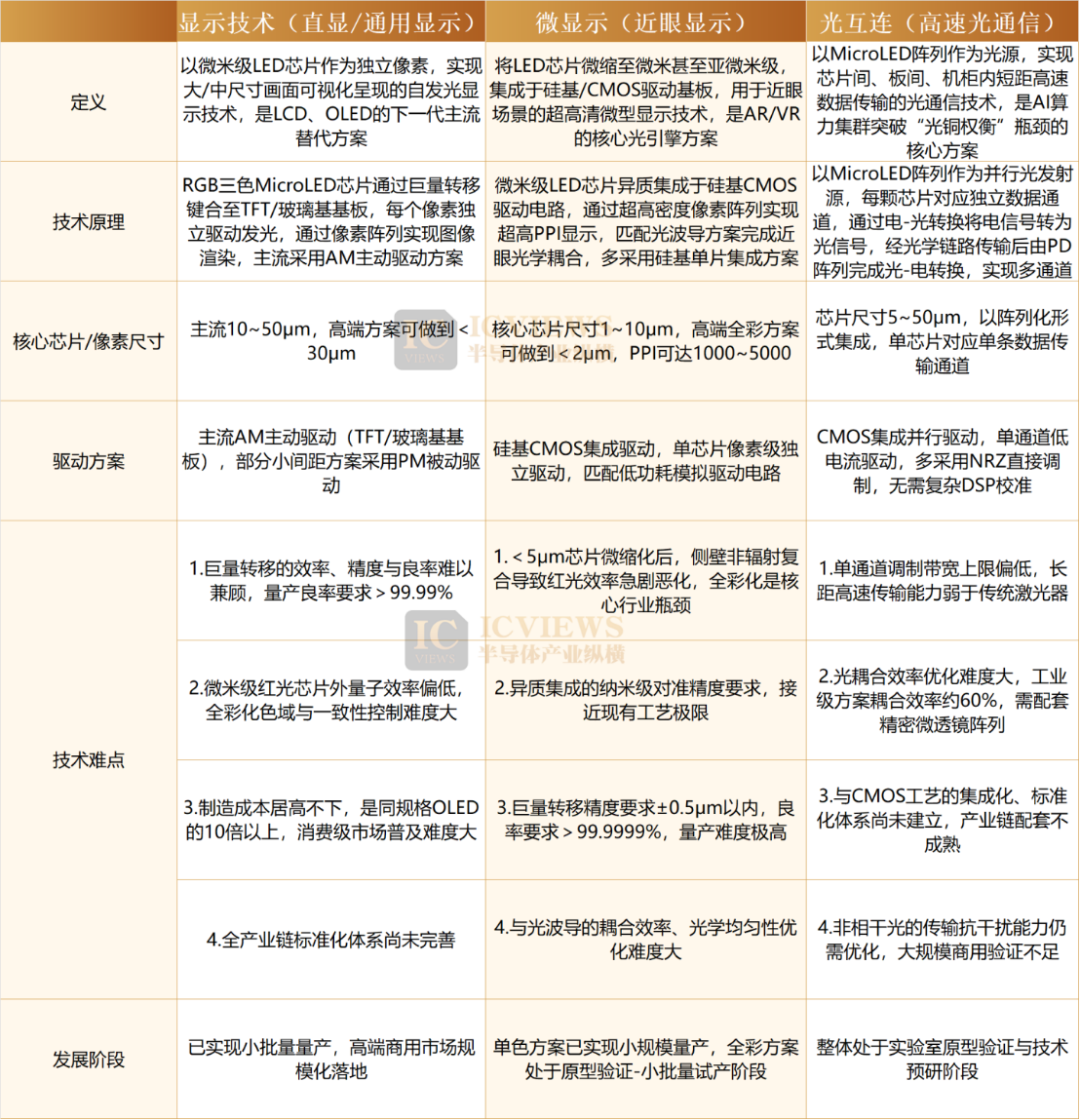
In display applications, each display pixel is composed of three independent micron-scale LED chips in red, green, and blue, each of which can be independently controlled by the drive circuit in terms of power-on state and luminance. Pixels that are not emitting light can be completely powered off, achieving true pure black display and completely avoiding the light leakage issue of LCDs. At the same time, the minimalist structural design removes the backlight, liquid crystal layer, and polarizer of LCDs, as well as the organic light-emitting layer of OLEDs, significantly improving light efficiency, stability, and integration, and also giving it the potential for cross-track applications.
02
Breaking the Dilemma of Choosing Between Optical and Copper, MicroLED Unlocks New Possibilities for 1.6T+ Ultra-High-Speed Interconnects
The explosive growth of current AI computing power has placed unprecedentedly stringent requirements on the interconnect bandwidth, transmission distance, power consumption, and reliability of data centers. However, traditional interconnect solutions have always been unable to escape the fundamental dilemma of choosing between "optical and copper" and struggle to adapt to the needs of computing power upgrades.
Specifically, although copper cable links have the advantages of high energy efficiency and strong reliability, they have a natural shortcoming in transmission distance—passive copper cables have a transmission distance of less than 2 meters, and active copper cables can only be extended to 5-7 meters. Moreover, as the bandwidth rate increases, issues such as signal attenuation, electromagnetic interference, and crosstalk will sharp (jījí, dramatically) intensify, making them unable to adapt to long-distance, high-speed transmission scenarios. Traditional optical links can achieve longer transmission distances but at the cost of high power consumption and low reliability. The power consumption of a single laser for communication can reach tens to hundreds of milliwatts, and large-scale array deployment will bring unbearable power consumption and heat dissipation pressure. At the same time, the complexity of multi-laser packaging will increase the failure rate, and reliability cannot be improved through redundant design. In scenarios with rates of 1.6T/3.2T and above, this dilemma of having to choose one or the other becomes increasingly prominent, becoming a key bottleneck restricting the scale expansion of computing power networks.
In contrast, MicroLED optical modules, leveraging their natural advantages in materials and architecture, achieve a combination of long-distance transmission, low power consumption, and high reliability, becoming an ideal light source to replace copper cables and complement traditional laser solutions, especially showing strong application value in the co-packaged optics (CPO) scenarios of AI data centers. Compared with traditional laser solutions, the core advantages of MicroLED optical modules are mainly reflected in five aspects:
First: Ultra-Low Power Consumption, Solving the Heat Dissipation Pain Point in High-Speed Scenarios
As a surface-emitting light source, MicroLED adopts an innovative "Wide and Slow (WaS)" architecture, abandoning the design concept of "a few high-speed channels" in traditional solutions and instead achieving high bandwidth through massive parallel transmission of low-speed channels. The essence of this architecture is to replace serial high-speed channels with parallel low-speed channels. For example, to achieve an 800G bandwidth, it can be completed through 400 channels with a single-channel rate of 2G in parallel, and the power consumption of light emission per channel is extremely low. The latest research data from IEEE's top journal in the field of photonics shows that for short-distance optical interconnect solutions based on MicroLED, the power consumption per channel can be reduced to 1/10 of that of traditional VCSEL solutions and 1/5 of that of silicon photonics solutions, while the integration density of the optical engine can be increased by more than 3 times, fundamentally solving the power consumption and heat dissipation pain points in high-frequency scenarios.
Second: Ultra-High Reliability, Approaching Copper-Grade Stability Standards
MicroLED chip sizes can be as small as 10 microns or even smaller, enabling large-scale array integration within a single optical module and easy deployment of redundant chips. For example, 400 channels can meet the 800G transmission demand, but 500 chips can actually be deployed. Even if 10% of the chips fail, it can still stably ensure 800G bandwidth transmission. This redundant design makes its reliability approach that of copper cables, completely solving the industry pain point of the failure rate of traditional laser solutions increasing synchronously with multi-channel deployment.
Third: Super Strong Bandwidth Expandability, Adapting to the Evolutionary Needs of 1.6T/3.2T Computing Power
The bandwidth improvement of MicroLED optical modules can be linearly expanded through two paths: "increasing the number of channels" and "increasing the single-channel rate" without the need for disruptive adjustments to the core architecture. Ultra-high-speed rate requirements such as 800G, 1.6T, and even 3.2T can be easily met by flexibly adjusting the channel scale, perfectly adapting to the continuous upgrade needs of the bandwidth of AI computing power networks.
Fourth: Full Ecosystem Compatibility, Seamlessly Connecting to Existing Network Architectures
MicroLED optical modules do not need to change the existing industry ecosystem and can directly adapt to standard interfaces such as OSFP and QSFP, as well as mainstream electrical host interfaces such as PCIe and VSR/MR, and mainstream protocols such as Ethernet, InfiniBand, NVlink, and CXL. They can directly replace existing optical and copper links without any modifications to existing hardware such as servers and switches, supporting hybrid deployment of copper and optical cables, significantly reducing the threshold and cost of technology implementation.
Fifth: Naturally Adapting to CPO Heterogeneous Integration, Fitting the Next-Generation Optical Interconnect Trend
MicroLED has natural advantages of micron-scale light-emitting size, high modulation bandwidth, low threshold current, and two-dimensional array integration, which deeply match the heterogeneous integration needs of CPO (co-packaged optics). Unlike traditional lasers that require complex temperature control and wavelength stabilization designs, MicroLED has a simpler structure and higher integration. It can be directly co-packaged with switching chips and ASIC chips without high-speed signal conversion, providing a minimalist and efficient solution for next-generation high-density computing power interconnection.
03
International Manufacturers Take the Lead: Accelerating the Industrialization of MicroLED Optical Interconnects
With its breakthrough technological value in the field of optical interconnects, MicroLED has attracted intensive layouts from enterprises upstream and downstream of the global industrial chain. International leading enterprises have taken the lead in making efforts, increasing investment in technology research and development and industrialization, and promoting the industry to quickly move from laboratory technology verification to commercial implementation.
Tech giant Microsoft has taken the lead in completing the prototype verification of the core architecture and introduced an architecture named MOSAIC (full name: MicroLED Optical System for Advanced Interconnects). Based on the "Wide and Slow" design concept and MicroLED light sources, this architecture achieves long-distance, low-power-consumption, and high-reliability signal transmission. It has completed prototype verification and successfully passed Ethernet and InfiniBand protocol stack tests, while also confirming compatibility with new protocols such as NVlink and CXL. Simulation data shows that the transmission distance of mass-production-grade modules can exceed 50 meters, and the power consumption is significantly reduced compared to traditional optical links.
The wafer foundry leader TSMC has reached in-depth cooperation with the US startup Avicena to jointly produce interconnect products based on MicroLED, replacing traditional electrical connections with optical communication. They focus on the core advantages of low cost and high energy efficiency, precisely matching the high communication needs of GPU clusters and directly addressing the interconnect bottleneck in AI computing power scenarios.
Chip design manufacturer MediaTek has independently overcome MicroLED light source technology and developed a new active optical cable (AOC) solution, which is expected to be officially unveiled at the Optical Fiber Communication Conference (OFC) in April this year. At the same time, its newly launched next-generation customized ASIC design platform can provide transmission interface solutions for heterogeneously integrating electronic and optical signals, precisely targeting the AI and high-speed computing markets.
AU Optronics in the panel field, relying on 30 years of glass process experience and combining its mature MicroLED mass transfer technology, has officially entered the short-distance optical communication market for AI data centers, achieving a cross-border extension from display technology to the field of optical communication.
In addition, professional interconnect technology enterprise Credo Technology has strengthened its optical interconnect technology capabilities by acquiring Hyperlume and is collaborating with enterprises such as Microsoft to promote the research and development and implementation of MicroLED optical interconnect technology, further expanding the boundaries of its application scenarios.
04
Domestic Enterprises Make Efforts: Multiple Breakthroughs Across the Entire Industrial Chain, Catching Up Simultaneously
While international manufacturers are accelerating technology implementation, domestic industrial chain enterprises are also quickly following up, achieving multiple breakthroughs in core chip research and development, module mass production, scenario verification, and other links, jointly promoting the industrialization process of MicroLED optical interconnect technology with international manufacturers.
In terms of core technology breakthroughs and industrialization implementation, many domestic enterprises have achieved phased results. Mega Semiconductor has completed the research and development of light source chips for MicroLED optical interconnect CPO technology and entered the sample verification stage. Its 400G and 800G parallel optical transceiver modules have achieved small-batch production, taking the lead in achieving industrialization breakthroughs for some products. Sanan Optoelectronics, in collaboration with Tsinghua University and China Mobile, has made major breakthroughs in the field of MicroLED optoelectronic devices and high-speed optical communication, successfully developing MicroLED light source devices with high-speed modulation capabilities. Tests show that its 3dB modulation bandwidth is expected to exceed 7GHz, and the NRZ-OOK data transmission rate is expected to exceed 10Gb/s, completing the core verification of key technologies. Leyard has provided MicroLED optical module products to the Chinese Academy of Sciences to replace the original traditional optical transmission solution. Currently, the solution is in the research and verification stage, achieving the initial implementation of scenario pilots. New Vision Microelectronics has signed a strategic cooperation agreement with BOE HC SemiTek. The two parties will jointly tackle the research and development and production of MicroLED optical interconnect technology and optical modules. Currently, they are extending their existing MicroLED product technologies to the optical interconnect scenarios of intelligent computing centers and simultaneously carrying out evaluation and analysis of scenario systems and performance indicators.
At the same time, many manufacturers are also conducting technical feasibility evaluations and early-stage layouts to charge up (xù lì, build up strength) for subsequent technology implementation. Unilumin Group stated that its MicroLED optical interconnect technology is in the technical feasibility evaluation and research stage. It will dynamically plan the research and development path and resource allocation for this technology direction based on the technology maturity curve and changes in market demand. Jucan Optoelectronics has also carried out relevant technical layouts in the field of MicroLED and is currently in the stage of technology exploration and accumulation, which has not yet been applied in the CPO field. Subsequently, it will flexibly adjust the promotion rhythm according to technology maturity.
05
Conclusion
From in-depth technological research in the display field to cross-border breakthroughs in the optical interconnect track, MicroLED is opening up brand new (quán xīn de, brand-new) growth space in the era of AI computing power. With the continuous investment of enterprises across the global industrial chain, continuous breakthroughs in technology research and development, and the continuous acceleration of the industrialization process, MicroLED is expected to completely rewrite the technological landscape of data center interconnects and become one of the core underlying technologies supporting the continuous upgrade of AI computing power.
-
![]()
ByteDance, DJI, and Xiaohongshu Secure Top Three Positions Among China’s Fastest-Growing Unicorns
-
Tesla's in-car voice system in China is finally learning to 'understand human language'
-
![]()
Foreigners Are Amazed: Chinese Electric Vehicle Drive Systems Unveil Innovative 'Poses'
-
![]()
700,000 Brothers and the Future of Robots: Behind JD.com's 'Nirvana Plan'
-
![]()
Zhipu's Trillion-Dollar Valuation: A New Chapter for China's AI
-
![]()
Is Laifen, a 'Dyson Alternative' on the Rise, Now Ensnared by the 'Alternative Curse'?
-
![]()
Beyond Patents: Insta360 and DJI Compete in Retail
-
![]()
Piercing Through Industry Chaos: The Curtain Rises on Compliance for Autonomous Driving