Breaking Through at Light Speed: The 'Core' Battle of China's Optical Communication Industry in the AI Era (Part 1)
 03/19 2026
 672
672
By Qianyanjun
Source: Bowang Finance
In early 2026, the capital markets saw a burst of brightness. By January 31, leading optical module companies such as Zhongji Innolight and YOFC had released their 2025 annual earnings forecasts, with most reporting over 50% projected growth. Among them, YOFC expected a net profit attributable to shareholders of RMB 9.4 to 9.9 billion, representing a year-on-year increase of 231.24% to 248.86%. Zhongji Innolight led the industry with a projected net profit of RMB 9.8 to 11.8 billion, up 89.5% to 128.17% year-on-year. Against the backdrop of macroeconomic pressures, these results were particularly striking. Around the same time, across the ocean, an even more shocking (earth-shaking) announcement came: NVIDIA revealed a multi-year strategic agreement with optical communication giants Lumentum and Coherent, involving billions of dollars in procurement commitments and $2 billion in investments in each company to support R&D and capacity expansion. Following the announcement, the stock prices of both companies surged.
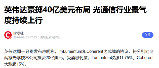
By the close of U.S. markets on March 2, Lumentum's stock had risen over 11%, while Coherent's had climbed over 15%. On one side, there was explosive growth in domestic earnings; on the other, an international AI leader was making a 'sky-high' bet on the upstream optical communication supply chain. Optical communication, once seen as a behind the scenes (behind-the-scenes) 'pipeline' in telecommunications networks, had suddenly moved to the forefront of the tech wave. This article delves into the inner workings of the supply chain, exploring its transformation from a 'pipeline' to a 'neural network,' and analyzing the opportunities and challenges for Chinese companies in this landscape.
01
The 'Moore's Law of Light': Technological Evolution Every Four Years
In the semiconductor industry, Gordon Moore's 'Moore's Law' predicted the doubling of transistors on integrated circuits every 18 months. In the optoelectronics field, a similar yet invisible 'Optical Moore's Law' exists: roughly every four years, optical module technology evolves to a new generation, halving the cost per bit and power consumption while doubling capacity. This law acts as an invisible baton, guiding the optical communication industry from 1.25 Gbps (gigabits per second, a common unit for measuring data transmission rates, representing one billion bits transmitted per second) to steady advancements toward 2.5 Gbps, 10 Gbps, 40 Gbps, 100 Gbps, and now to single-wavelength speeds of 100 Gbps, 400 Gbps, and even 1.6 Tbit/s in the ultra-fast era.
Each leap in speed relies on a tiny yet crucial component: the optical chip. It is the heart of the optical module, the foundation of optoelectronic signal conversion, and its performance directly determines the transmission efficiency of the entire communication system.
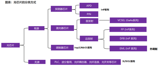
Figure: Source: Yuanjie Technology Prospectus, Fiber Online
Optical chips primarily fall into two categories based on function: First, laser chips responsible for 'electrical-to-optical' conversion, acting like precise telegraph operators that accurately convert electrical signals into optical signals for transmission. Second, detector chips for 'optical-to-electrical' conversion, functioning as loyal receivers that restore incoming optical signals to electrical signals.
The family tree of laser chips is quite complex. Based on emission type, they can be divided into surface-emitting and edge-emitting lasers. Surface-emitting lasers (SEL), represented by VCSELs (Vertical-Cavity Surface-Emitting Lasers), emit laser light perpendicular to the top surface, producing a circular beam with a small divergence angle, facilitating easy coupling and commonly used for short-distance transmission within data centers.
Figure: Schematic of surface-emitting laser chips
Consider a practical example: when you hold a phone to your ear during a call, the screen automatically dims; when you move it away, the screen brightens again. Behind this lies a proximity-sensing module powered by VCSEL chips—emitting low-power laser light that reflects when an object approaches, allowing the phone to detect proximity and adjust the screen accordingly.
Edge-emitting lasers (EEL) emit light parallel to the substrate surface and include three main types: FP (Fabry-Perot Laser), the earliest, used for low-speed, short-distance transmission, akin to a 'workhorse'—diligent but limited in capability. DFB (Distributed Feedback Laser) introduces a grating to the FP structure, achieving single-longitudinal-mode output, akin to adding 'noise reduction' to sound, suitable for high-speed, medium-to-long-distance transmission but prone to 'chirping' (a term describing the shift in center wavelength during pulse transmission, affecting quality). To address chirping, EML (Electro-Absorption Modulated Laser) emerged, integrating a DFB laser with an electro-absorption modulator for high-quality signal transmission, akin to a well-trained professional 'announcer,' clear and precise, becoming the top choice for high-speed backbone and metropolitan networks.

Figure: Schematic of edge-emitting laser chips
Among detector chips, PIN detectors dominate, offering moderate sensitivity and fast response, suitable for most conventional scenarios. APD (Avalanche Photodiode) detectors, by contrast, are like special forces with 'night vision' capabilities. They amplify weak optical signals through internal avalanche effects, achieving extremely high sensitivity, capable of detecting single photons, widely used in quantum communication and other fields requiring long-distance, high-sensitivity detection.
Whether evolving from FP to DFB to EML or from PIN to APD, each technological iteration aims to transmit more data over longer distances, at faster speeds, and with lower power consumption. This is the most fundamental driving force behind the 'Optical Moore's Law.'
02
The 'Neural Network' of AI Computing Factories: A Revolution on the Demand Side
If the past two decades of optical communication growth were primarily driven by telecommunications infrastructure construction (e.g., fiber-to-the-home, 4G/5G base stations), today, the core engine propelling its rapid expansion has shifted to artificial intelligence.
As NVIDIA founder and CEO Jensen Huang stated, 'The way we compute has fundamentally changed. In the AI era, software runs on intelligence, driven by tokens generated in real-time by AI factories for every interaction and context.' This massive 'AI factory' is essentially a supercomputer cluster composed of tens of thousands of GPUs (Graphics Processing Units) or TPUs (Tensor Processing Units). When training a trillion-parameter large model, data must be exchanged billions of times across tens of thousands of chips.
Under traditional schemes, data exchange relies on interconnects made of materials like aluminum, copper, or carbon nanotubes. As chip fabrication processes shrink, interconnects must become thinner, but reducing their spacing introduces physical limits for copper and increases parasitic effects between electronic components, becoming a bottleneck for computing power growth.
Optical interconnects offer an ideal solution. For example, as new energy vehicles become increasingly intelligent, beyond L3 autonomy, the number of screens, cameras, pixels, and resolutions in vehicles will further increase, demanding higher data exchange volumes and speeds. Copper-based automotive Ethernet architectures can no longer support high-load scenarios like multi-screen interaction, 4K/8K cockpit displays, and real-time AI inference in terms of bandwidth, weight, and anti-interference capabilities. Adding more copper cables is impractical, while fiber optics offer significant lightweight advantages, making them better suited for data exchange. The 'White Paper on In-Vehicle Optical Communication Technology' released by the Shenzhen Automotive Research Institute of Beijing Institute of Technology notes that in-vehicle fiber-optic communication can easily support data transmission rates of 10 Gbps and above, meeting future application growth, whereas copper links face electromagnetic interference challenges beyond 10 Gbps and are costly, with potential increases in copper demand also challenging vehicle energy efficiency per mile.
Thus, 'optical replacing copper' is no longer just a slogan in the communications industry but a highly certain and inevitable choice. The author believes that the two largest application scenarios for future optical modules will be in AI infrastructure, where optical pathways replace inter-chip data circuits to achieve high-capacity, energy-efficient interconnects—this is precisely why NVIDIA invested heavily in Lumentum and Coherent. The two sides will collaborate on developing next-generation silicon photonics technology to build AI infrastructure of unprecedented scale, speed, and energy efficiency.
This demand storm from AI is clearly reflected in market size projections.
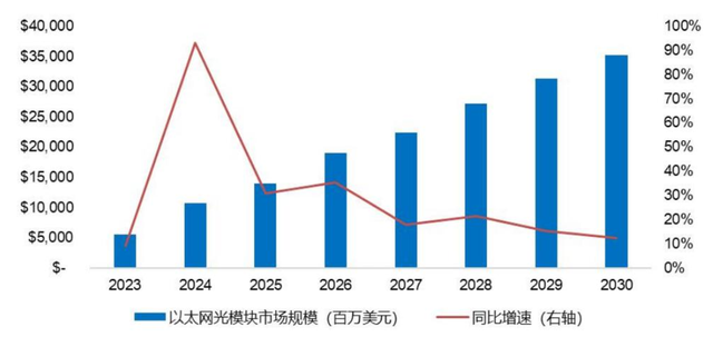
Source: Zhongji Innolight Announcement, Lightcounting
According to forecasts by optical communication market research firm Lightcounting, the global Ethernet optical module market is set for sustained rapid growth, reaching $18.9 billion in 2026, up 35% year-on-year, and expected to surpass $35 billion by 2030. The primary driver is strong demand for high-speed optical modules in AI infrastructure construction. As token generation by giants like OpenAI, Microsoft, and Google escalates, the number of accelerator chips needed for a single inference cluster is projected to reach the million level, far exceeding training clusters. Chip clustering will inevitably drive dual growth in both the quantity and speed of optical modules. NVIDIA's expansion of Rubin series network cards and Google's increased TPU array sizes all confirm this trend.
Guosheng Securities notes that the global optical module market could reach $24-28 billion by 2028, maintaining a compound annual growth rate of 12%-14.9% from 2023-2028.
Domestically, the automotive sector represents a blue ocean for optical module applications—using 'fiber-to-the-vehicle' to address bandwidth constraints in intelligent connected vehicles and promoting deep integration between the optoelectronics and automotive industries, both worth trillions of dollars. Industry expert Liu Wu argues that L3+ autonomous driving currently demands data transmission rates exceeding 100 Gbps, with fiber-optic sensing offering irreplaceable advantages in core areas like battery safety warnings. He projects China's in-vehicle high-speed communication and sensing market to reach the hundred-billion-dollar level by 2030.
It is clear that optical communication is no longer the obscure 'pipeline' but a core infrastructure in the AI era, acting as the 'neural network' that determines computing efficiency in intelligent vehicles. So, how are Chinese companies faring in the global optical communication landscape? We will continue this analysis in the next installment.
-
![]()
ByteDance, DJI, and Xiaohongshu Secure Top Three Positions Among China’s Fastest-Growing Unicorns
-
Tesla's in-car voice system in China is finally learning to 'understand human language'
-
![]()
Foreigners Are Amazed: Chinese Electric Vehicle Drive Systems Unveil Innovative 'Poses'
-
![]()
700,000 Brothers and the Future of Robots: Behind JD.com's 'Nirvana Plan'
-
![]()
Zhipu's Trillion-Dollar Valuation: A New Chapter for China's AI
-
![]()
Is Laifen, a 'Dyson Alternative' on the Rise, Now Ensnared by the 'Alternative Curse'?
-
![]()
Beyond Patents: Insta360 and DJI Compete in Retail
-
![]()
Piercing Through Industry Chaos: The Curtain Rises on Compliance for Autonomous Driving