Breaking Through at Light Speed: The 'Core' Battle in China's Optical Communication Sector in the AI Era (Part 3)
 03/27 2026
 585
585

By Qianyanjun
Source: Bowang Finance
In our previous discussion, we noted that domestic companies still have shortcomings in high-end optical chips. While this presents a challenge, it also points to the core direction for future technological breakthroughs and industrial investment. The author believes that to win this critical battle, two clear paths exist: one is to fully invest in the next-generation disruptive technology—silicon photonics—and the other is to return to the essence of the industry by embracing the IDM model.
01
Breaking the Deadlock: Opportunities in Silicon Photonics Technology and the IDM Model
In high-end optical modules, optical chips account for nearly 50% of the cost, making them key determinants of product performance and cost. The raw materials for optical chips are primarily semiconductor materials, commonly using III-V compounds such as indium phosphide (InP) and gallium arsenide (GaAs) as substrate materials. Traditional optical modules can modulate and receive optical signals, comprising optical transmitters, receivers, and optical chips, among other components, integrated using packaging technology on an InP substrate. Silicon photonics technology, on the other hand, leverages mature silicon-based CMOS processes to integrate optical devices on silicon-on-insulator (SOI) wafers, achieving 'optoelectronic integration.' It is seen as a promising way to break the monopoly of III-V semiconductor materials (such as InP and GaAs). This represents not just a change in technological approach but a dimensional reduction in the industrial ecosystem.
The advantages of silicon photonics technology are disruptive: First, it has significant cost potential. The price of a silicon substrate is only about $0.2/cm², while an InP substrate is more than 20 times as expensive. Moreover, silicon photonics can leverage mature, high-capacity CMOS production lines, further highlighting its advantage of low cost at scale. Second, it offers high integration. The high refractive index of silicon allows for a significant reduction in the bending radius of optical waveguides, enabling the high integration of modulators, receivers, and passive optical components on a single chip. Third, it achieves high process precision. The process precision range for silicon photonics chips is 65nm-250nm, while traditional InP technology typically ranges from 300nm-500nm. The yield rate for silicon photonics chips can exceed 80%, whereas traditional solutions often have a yield rate below 40%.
According to data from French market research and consulting firm YOLE, the global market size for silicon photonics chips is projected to reach $970 million by 2027, with a compound annual growth rate (CAGR) of 36.2% from 2021 to 2027. Currently, silicon photonics technology is in its second stage of development, transitioning from hybrid integration to monolithic integration. The ultimate goal for the future is to achieve full optoelectronic functional integration and even programmable chips.
In the international market, Intel and Cisco are the dual oligopolies in the silicon photonics field, collectively occupying approximately 88% of the global silicon photonics module market share. However, the author observes that in the Chinese market, a 'whole-industry-chain mobilization' targeting silicon photonics has already begun. From upstream SOI substrates (Shanghai Simgui, controlled by National Silicon Industry Group) to midstream chip design and manufacturing (Chongqing United Microelectronics Center CUMEC, Shanghai Industrial μTechnology Research Institute SITRI), and then to packaging and testing (TFC Communication, ficonTEC, in which Robotech has a stake), a complete domestic silicon photonics ecosystem is taking shape at an accelerated pace.
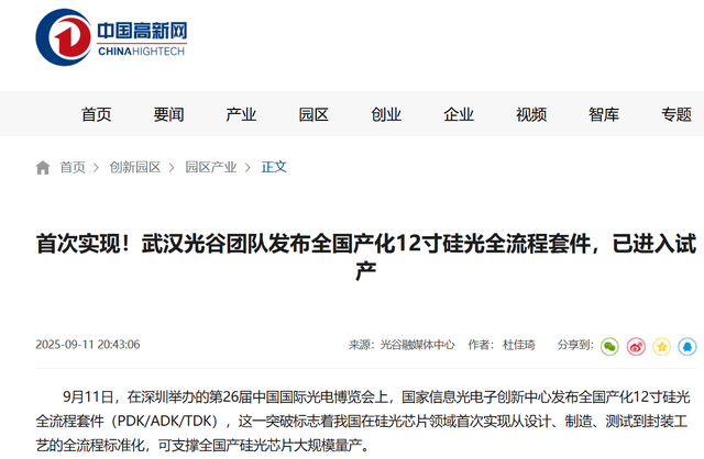
In September 2024, the National Information Optoelectronics Innovation Center released a fully localized 12-inch silicon photonics full-process kit (PDK/ADK/TDK), achieving full-process standardization from design to packaging for the first time and paving the way for large-scale production.
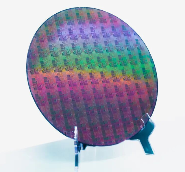
Figure: A 12-inch silicon photonics chip produced using the full-process kit
In the new track (translated as 'arena' or 'field') of silicon photonics, the gap between China and the world is much smaller than in the traditional high-end optical chip field, providing a valuable time window for 'overtaking.'
2. The IDM Model: The Inevitable Path to Industrial Maturity
For optical chips, which are 'specialty process' products, value enhancement does not rely solely on size reduction but more on the deep coupling of materials, processes, and design. Therefore, compared to the Fabless model prevalent in logic chips, the IDM model is the mainstream and direction for the optical chip industry.
New entrants in the logic chip sector often adopt the Fabless model to reduce capital expenditures. The IDM model ensures autonomous control over production capacity, shortens product development cycles, enables rapid response to customer needs, and allows for quick identification of design or process issues, facilitating efficient iteration. Especially during the reliability verification phase of high-end optical chips, the advantages of the IDM model are irreplaceable. Faced with complex verification processes lasting thousands of hours, IDM manufacturers can master every vertical production link from design conversion to manufacturing, adjusting production parameters in real-time based on test results for the next round of tape-outs. In contrast, Fabless manufacturers must repeatedly communicate with foundries, significantly reducing efficiency.
Domestic companies aspiring to climb the peak of high-end optical chips, such as Yuanjie Technology and Shijia Photonics, are all developing the IDM model and striving to master core processes like epitaxial growth. This is a capital-intensive path with a long return cycle, but it is also the only route to the top of the industrial chain. The flexibility of the 'light' model cannot ultimately replace the depth of the 'heavy' model. When the tide goes out, we see who is swimming naked; when the industry enters deep waters, we see who has mastered core technologies.
02
'Light Catchers' at the Forefront: Analysis of Potential Targets
Based on the above analysis, in the golden track (translated as 'arena' or 'field') of optical communication, three types of companies warrant investors' close attention:
Type 1: Global Leaders, the 'Ballast Stones' of Performance Release
Companies like Zhongji Innolight and New Sailor represent this category. They have already proven their industry position and profitability with better-than-expected performance (as analyzed in our previous article). They are not only the biggest beneficiaries of the current AI computing power wave but also pioneers in new technologies (such as 1.6T optical modules and silicon photonics modules). Their strong cash flow and scalable manufacturing capabilities provide solid support for penetrating upstream into the chip sector and integrating the industrial chain. For conservative investors, they are a good choice to share in the industry's determinism (translated as 'certain') growth.
Type 2: Silicon Photonics Newcomers, the 'Game Changers' in Core Technologies
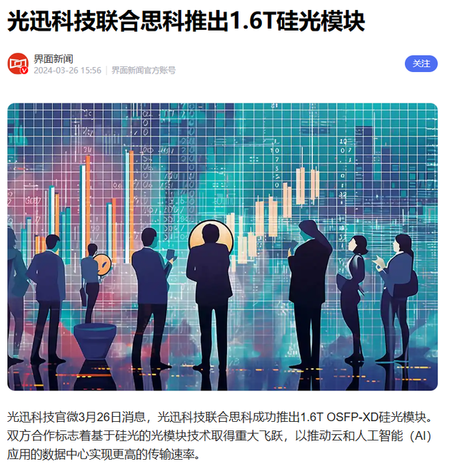
These companies represent hope for breaking through the 'chip shortage' bottleneck. Accelink Technology, an established giant in optical devices, has achieved self-research in core optical chips such as CW lasers and detectors and has launched a 1.6T silicon photonics module in collaboration with Cisco, demonstrating strong comprehensive strength.
Shijia Photonics has achieved breakthroughs in core light sources, with its high-power DFB lasers already shipped in small batches, providing critical component support for domestic silicon photonics modules. The increase in its overseas market revenue also confirms the competitiveness of its products. Yuanjie Technology is a pure play in high-end optical chips. Despite facing challenges, each of its technological breakthroughs is significant. Additionally, Robotech (with a stake in ficonTEC) and TFC Communication, which provide key equipment and packaging in the silicon photonics ecosystem, also possess scarce value.
Type 3: Cross-Industry Pioneers, the 'Pioneers' of Application Scenarios
These companies are opening up a second growth curve for optical communication. Amid the trend of 'optical-vehicle integration,' Yangtze Optical Fiber and Cable and HG Tech, leveraging their deep accumulation in fiber optic cables and optical devices, have taken the lead in 'boarding the vehicle' and sharing in the dividends of automotive intelligence. Meanwhile, Evergreen Ecology has entered the optical module field through restructuring and controlling Wuhan Junheng, with Coherent as its largest customer, demonstrating deep integration with the global industrial chain. Their growth will complement the traditional communication sector and build a more solid business foundation.
Epilogue: Illuminating the 'Optical Foundation' of the Intelligent Era
From a 'pipeline' connecting the world to the 'neural network' of AI computing power factories, and then to the 'nerve endings' of intelligent vehicles, the value boundaries of optical communication are expanding at an unprecedented pace. This is not just a technological evolution but a leap in industrial status.
Looking back at this 'light-speed breakthrough,' we see Chinese companies continuously striving for progress, gaining dominance in the global midstream manufacturing sector. We also see calmness and urgency in the core upstream sector—the mere 4% localization rate of high-end optical chips represents both an opportunity and a 'Loushanguan Pass' that must be crossed. The rise of silicon photonics technology provides China with a rare opportunity to change lanes; the return to the IDM model reflects a profound understanding and practice of industrial laws.
The author believes that future investment is essentially an investment in trends and scarcity. The trend in optical communication is the endless demand for AI and computing power; its scarcity lies in high-end optical chips, advanced silicon photonics technology, and the comprehensive barriers formed under the IDM model. When an industry possesses both 'Beta of the Times' and 'Alpha of Effort,' its explosive potential cannot be ignored.
As NVIDIA envisions, future AI factories will be driven by real-time-generated tokens. It is the invisible yet rock-solid 'optical foundation' woven by countless optical modules and chips that will carry these massive tokens and make intelligence ubiquitous. This light not only illuminates the path of data but also lights up China's technology industry (translated as 'technology industry') journey from a manufacturing powerhouse to an intelligent manufacturing powerhouse. In this race for the future, whoever masters the core 'light' and the underlying 'chips' will navigate steadily and far in the vast sea of the intelligent era.
-
![]()
ByteDance, DJI, and Xiaohongshu Secure Top Three Positions Among China’s Fastest-Growing Unicorns
-
Tesla's in-car voice system in China is finally learning to 'understand human language'
-
![]()
Foreigners Are Amazed: Chinese Electric Vehicle Drive Systems Unveil Innovative 'Poses'
-
![]()
700,000 Brothers and the Future of Robots: Behind JD.com's 'Nirvana Plan'
-
![]()
Zhipu's Trillion-Dollar Valuation: A New Chapter for China's AI
-
![]()
Is Laifen, a 'Dyson Alternative' on the Rise, Now Ensnared by the 'Alternative Curse'?
-
![]()
Beyond Patents: Insta360 and DJI Compete in Retail
-
![]()
Piercing Through Industry Chaos: The Curtain Rises on Compliance for Autonomous Driving