In Jiaxing, more than 600 experts discussed the future of lithography
![]() 10/17 2024
10/17 2024
![]() 526
526
Lithography technology is the core process of semiconductor manufacturing, determining the integration and performance of chips. In the vast universe of chip manufacturing, lithography technology is undoubtedly one of the brightest stars, leading the innovation and frontier development of the entire industry.
In recent years, the integrated circuit industry has become increasingly important in countries around the world and has become a strategic industry that all countries attach great importance to. Based on this situation, the International Workshop on Advanced Patterning Solutions (IWAPS) came into being. Since 2017, IWAPS has been successfully held for seven consecutive years.
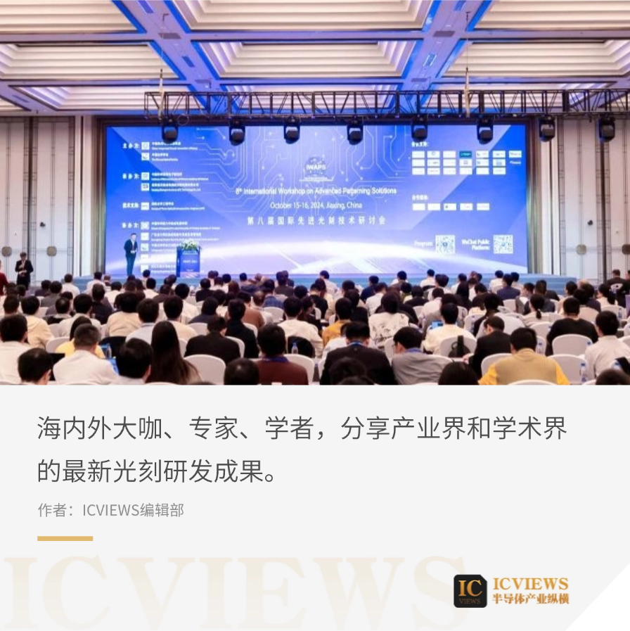
Today, the 8th International Workshop on Advanced Patterning Solutions (IWAPS) was held in Jiaxing, Zhejiang Province. This year's IWAPS was hosted by the China Integrated Circuit Innovation Alliance, the Chinese Optical Society, and SPIE - The International Society for Optical Engineering. It was undertaken by the Institute of Microelectronics of the Chinese Academy of Sciences and Nanjing Chengxin IC Technology Research Institute Co., Ltd. It was co-organized by the School of IC, University of Chinese Academy of Sciences, Guangdong-Hong Kong-Macao Greater Bay Area Institute of IC and System Applications, the Lithography Technology Professional Committee of the Chinese Optical Society, Zhejiang Provincial Investment Group Co., Ltd., and Zhejiang Xinsen Semiconductor Technology Co., Ltd. More than 600 experts, scholars, entrepreneurs, and young scholars from numerous domestic and foreign scientific research institutions, universities, and renowned enterprises gathered together.
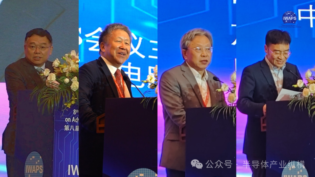
Wei Yayi, Secretary-General of the organizing committee, professor at the University of Chinese Academy of Sciences, researcher at the Institute of Microelectronics of the Chinese Academy of Sciences, and SPIE Fellow, presided over the meeting. IWAPS Chairman, Cao Jianlin, Director of the China Integrated Circuit Innovation Alliance, and researcher, Gu Bo, Deputy Secretary-General of the Chinese Optical Society, Fellow of the Canadian Academy of Engineering, Fellow of the Chinese Optical Society, Fellow of the Optical Society of America, SPIE Fellow, and Fellow of the Laser Institute of America, Li Ling, Deputy Director and researcher at the Institute of Microelectronics of the Chinese Academy of Sciences, and Deputy Dean of the School of IC, University of Chinese Academy of Sciences, attended the opening ceremony and delivered speeches.
Wei Yayi, professor at the University of Chinese Academy of Sciences, researcher at the Institute of Microelectronics of the Chinese Academy of Sciences, and SPIE Fellow, presided over the meeting. He said that in this ever-changing and complex world, there are many uncertainties. In this context, academic exchanges are crucial for technological innovation, especially in the field of patterning technology, to strive to solve these problems. Over the past few years, the IWAPS has continued to grow and expand. Since the first workshop, the number of participants and papers submitted has continued to increase. This year, a partnership has been established between IWAPS and SPIE to promote the development of leading institutional software and patterning technology as well as global calibration.
IWAPS Chairman, Cao Jianlin, Director of the China Integrated Circuit Innovation Alliance, and researcher, shared three insights.
Firstly, this year's IWAPS is the eighth session, and the venue is chosen in South Lake, Jiaxing, a name familiar to every Chinese. It was here that the Communist Party of China embarked on its journey. When the forefathers founded the Communist Party of China here, they were determined to overthrow the reactionary rule and build a new, democratic, free, prosperous, and powerful China. In the early 21st century, the most complex process in advanced integrated circuit technology, Patterning technology or Lithography technology, requires equipment that is the most complex in the entire front-end lithography process. Many Chinese people are continuously working hard on this. I believe that the IWAPS will continue to be held session after session in the future, and experts, entrepreneurs, and scholars like today's participants will gather here.
Secondly, the significant impact of SPIE (The International Society for Optical Engineering) on China's scientific and technological community. More than 30 years ago, SPIE was still discussing whether some Chinese students could be introduced to participate in its conferences for developing countries like China. Today, I hope everyone will continue to promote engineering optics and advanced technology worldwide. Engineering science and technology, including related research and industry, should benefit all mankind. We hope that our cooperation with SPIE will be successful and attract more international friends here next year.
Thirdly, the world is currently facing some economic difficulties, and countries are seeking solutions. This year's Nobel Prizes in Physics and Chemistry were awarded to AI, while the Prize in Economic Sciences was awarded to economists studying the relationship between economic development and institutions. I think this is excellent. China's development path with Chinese characteristics is also worthy of study and discussion by global economists. The relationship between technological development, economic development, and institutions is complex and does not belong solely to a particular institution. I believe that the Chinese people and Chinese scientists will prove through practice that China's development path with Chinese characteristics is effective, and we can quickly narrow the gap with developed countries and move to the forefront of global technological development. I believe that in the field of Patterning technology or Lithography technology, China will surely flourish rapidly.
Gu Bo, Deputy Secretary-General of the Chinese Optical Society, Fellow of the Canadian Academy of Engineering, Fellow of the Chinese Optical Society, Fellow of the Optical Society of America, SPIE Fellow, and Fellow of the Laser Institute of America, said that currently, there are many limitations and obstacles to the development of advanced lithography technology in China. However, this also provides many opportunities for researchers in this field. I hope everyone can closely integrate their personal research with the actual needs of the country and truly serve the development needs of China's integrated circuit industry. We also need to keep abreast of the latest developments in technologies such as ultra-precision, deep ultraviolet (DUV), and extreme ultraviolet (EUV) optics. AI-assisted technology, GPU acceleration technology, and more. These technologies will help and accelerate technological development in this field, especially AI technology.
Li Ling, Deputy Director and researcher at the Institute of Microelectronics of the Chinese Academy of Sciences and Deputy Dean of the School of IC, University of Chinese Academy of Sciences, said that the microfabrication of integrated circuits following Moore's Law has already faced challenges, with the physical limits of transistors increasingly approaching. Meanwhile, the demand for low-power and high-performance chips is becoming more urgent, placing tremendous pressure on the development of lithography technology. In this context, strengthening international cooperation and interdisciplinary collaboration to jointly promote the advancement of lithography technology is bound to have a profound impact on human development. This conference focuses on the forefront of lithography technology, providing an important exchange platform for the domestic and foreign semiconductor industry and academia. Participants shared research results, explored patterning solutions, and discussed upcoming technical challenges around themes such as materials, equipment, measurement, software, and design, which is also of great significance in promoting international exchanges, disciplinary development, and industry-university-research cooperation.
01
The Voice of Lithography Conference
Since its inception in the 1960s, lithography technology has undergone several innovations, driving the advancement of chip manufacturing processes from initial micron-level patterns to today's nanometer-level processing.
Lithography equipment, processes, inspection and metrology, masks and materials... During the two-day conference, experts and scholars in the field of lithography technology from home and abroad will take turns to share their new breakthroughs in various frontier topics, display academic achievements, and announce technological development achievements and products.
Hong Xiao, Senior E-Beam and Process Expert at ASML, shared the signal enhancement of scanning electron microscopy (SEM) for buried patterns and defects.
The enhanced backscattered electron (BSE) image of buried structures is obtained by removing low-energy (<100 eV) secondary electrons (SE) and high-energy elastic backscattered electrons (EBSE) in scanning electron microscopy (SEM). Secondary electrons and elastic backscattered electrons originate from the sample surface and thus do not contribute to buried structure imaging and buried defect detection. We used an electron beam inspection (EBI) system with a high-pass energy filter (EF) to image 300 mm all-around gate (GAA) nanosheet (NS) structures with different residual silicon germanium. It was successfully demonstrated that by adjusting the settings of the energy filter, the backscattered electron imaging of buried silicon germanium can be improved, and this technique can be applied to other buried structure imaging and buried defect detection.
Billy Tang, Marketing Manager at ASML subsidiary Cymer, shared improvements in sustainability and usability brought about by advancements in light source technology. ASML is committed to sustainability across the organization, aiming for net-zero emissions from ASML operations/manufacturing, business travel, and commuting by 2025, a net-zero supply chain by 2030, and net-zero emissions from product use by 2040.

Billy Tang said that sustainability and usability improvements are our core concerns, requiring simultaneous reductions in environmental impact and improvements in light source efficiency and overall performance. This discussion introduces software for automatic data analysis and performance tuning (ADAPT), an AI-driven product.
Since the introduction of its first-generation ArF light source, Cymer has improved energy efficiency through its dual-chamber (MOPA) technology. The chamber and ADAPT technology contribute to efficiency gains by further reducing power consumption.
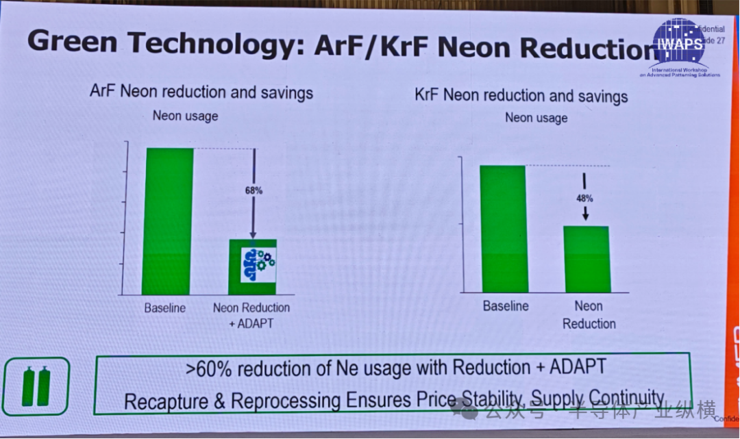
Based on these AI algorithms, ASML has established specific standards for each system, which can vary even within the same system or chamber over its lifetime, such as within a year. Therefore, we use adaptive algorithms to enable certain automation equipment to intelligently sense its own materials.
With this, the performance of the machine itself can be optimized. And various energy savings can be achieved through the use of adapters, starting with the first reduction in neon gas, which is used in the gas chamber. Therefore, with the support of ADAPT and our neon emission reduction technology over the past few years, we can reduce neon usage by more than 60%. Now on ADAPT+ArF, we can achieve a reduction of approximately 60% or more, which helps customers obtain guaranteed prices and supply.
Liu Yang from Harbin Institute of Technology shared intelligent ultra-precision motion control technology for lithography equipment. He said that for step-and-scan projection lithography machines, the synchronous servo performance of the mask stage and wafer stage will directly affect the technical indicators of the lithography machine. The mask stage and wafer stage are typical six-degree-of-freedom ultra-precision motion platforms. The core control problem is to balance high dynamics and ultra-precision motion under coupled dynamics and complex internal and external disturbances. The research and development of ultra-precision motion platform control technology for integrated circuit lithography machines is of great significance for realizing the localization of high-end lithography machines.
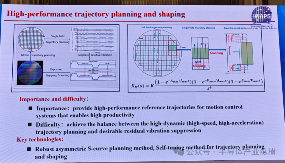
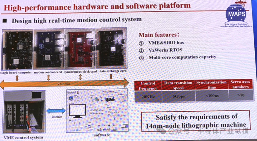
In this report, he first described the servo performance requirements of high-end lithography ultra-precision motion platforms and the technical challenges faced in meeting these requirements. Then, he introduced the research results and latest progress in the control of lithography ultra-precision motion platforms from five aspects: decoupling control, feedback control, feedforward control, trajectory generation, and collaborative control. Finally, existing problems and development trends were discussed.
Hong Chen from the National Microelectronics Institute shared research on the importance of mask thickness effects on 28 nm and below nodes. As feature sizes in semiconductor manufacturing approach 28 nm and smaller, the impact of mask thickness in lithography becomes increasingly significant, leading to critical dimension (CD) variations and edge placement errors (EPE), collectively known as three-dimensional effects.
The effects of mask three-dimensional effects mainly stem from three factors: absorber topography coupling, electromagnetic field changes caused by mask structure, and lithography-induced shadowing effects. These effects pose challenges to traditional mask correction tools and pose risks to maintaining high yields in chip production.
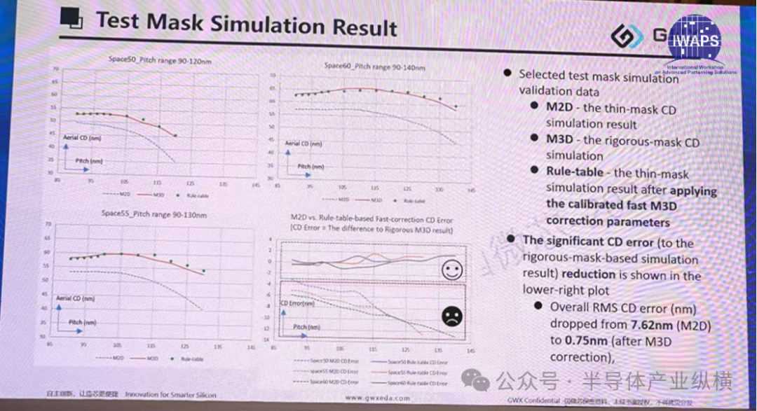
More accurate modeling with the ability to capture and correct three-dimensional thickness effects is crucial for generating mask data to perform the intended lithography imaging process with high-fidelity features. This can achieve two goals: (1) generating patterns as close as possible to the design intent; (2) maximizing the process window (PW) with the combination of RET and OPC technologies.
The research work will proceed in the following three parts in sequence: (1) Conduct a comprehensive and complete research investigation on deviations in CD and EPE under various pre-designed process conditions; (2) Select the most typical and representative complex mask near-field transmission scenarios for research and compare them with situations in the "Kirchhoff" domain; (3) Summarize and derive the effects obtained from selected correction methods with higher complexity, providing more realistic and practical insights into how to balance the required accuracy and operational performance in mask data optimization based on full-chip OPC.
Dejian Li from UMC shared an overview of lithography printability assessment in mature node photomask manufacturing. In the photomask manufacturing process, it is mainly divided into patterning and quality control processes. Inspection, repair, and AIMS (Automatic Image Measurement System) can ensure that the mask is defect-free.
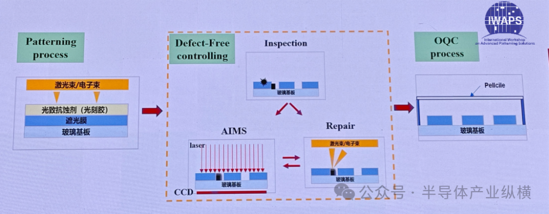
To improve the efficiency of our mature mask manufacturing and reduce cycle time, lithography printability assessment (LPR) has been introduced as an effective defect handling method and can serve as a valuable supplement or alternative to the AIM system.
In PDM masks, LPR demonstrates high efficiency in both L/S (line and space) and CT (contact hole) PDM defects and shows a good linear relationship with AIMS, without missing critical defects. For L/S and CT patterns, the gap between AIMS results and LPR results is within 2% within the range of critical dimension deviation (CDE) less than ±15%.
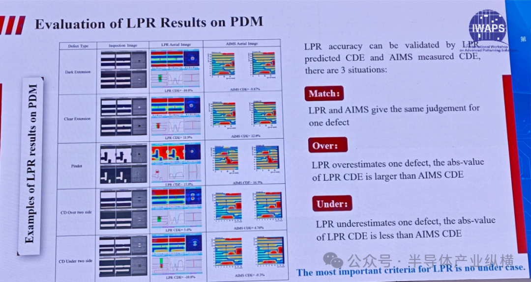
So, if 10% CDE results from AIMS are used as the criterion for determining whether a defect needs to be repaired, 8% can be used as the threshold for LPR to determine whether a defect passes. In production masks, most defects can be filtered out without AIMS printability confirmation, which improves cycle time and efficiency in mask manufacturing.
