Chengfeng Technology Shines at CIOE 2026: Bolstering the ‘Chinese Core’ of AI Optical Interconnection with Cutting-Edge Nanoscale Optical Inspection
 09/16 2026
 473
473
From September 9 to 11, 2026, the 27th China International Optoelectronic Exposition (CIOE 2026) was held with great fanfare at the Shenzhen International Convention and Exhibition Center. Under the theme of ‘AI Empowers New Transformations in Optoelectronics,’ the event drew over 4,000 top-tier exhibiting enterprises from across the world.
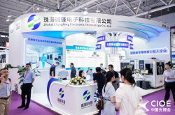
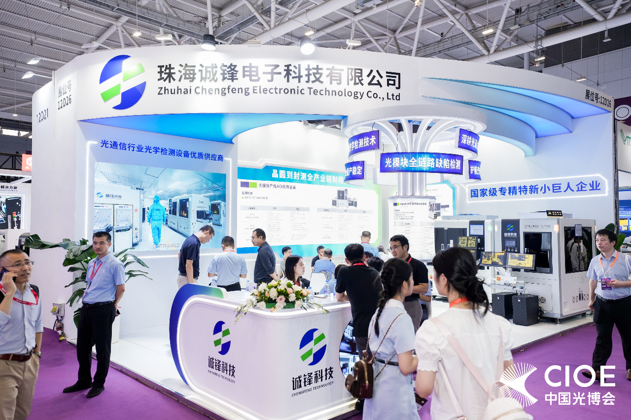
At this grand annual gathering of the optoelectronics industry, Zhuhai Chengfeng Electronic Technology Co., Ltd. (hereinafter referred to as ‘Chengfeng Technology’), a national-level ‘Little Giant’ enterprise specializing in sophisticated and innovative solutions, made a remarkable presence with its comprehensive optical inspection solutions tailored for the entire optical communication industry chain. At booth 12D26, it showcased its latest advancements in the field of optical communication inspection.
Currently, the exponential growth of AI computing power is fueling a surge in demand for high-speed optical interconnection. Amid the trend of ‘optical advancement and electrical retreat,’ the mass production of CPO (Co-Packaged Optics) and silicon photonics has emerged as a core focus within the optoelectronics industry. Optical modules are rapidly evolving from 400G to 800G and 1.6T, accompanied by an increase in the complexity of packaging processes. Consequently, numerous sub-micron-level inspection needs have arisen at various process stages, posing challenges for traditional semiconductor AOI (Automated Optical Inspection) equipment to keep pace with the industry's rapid development.
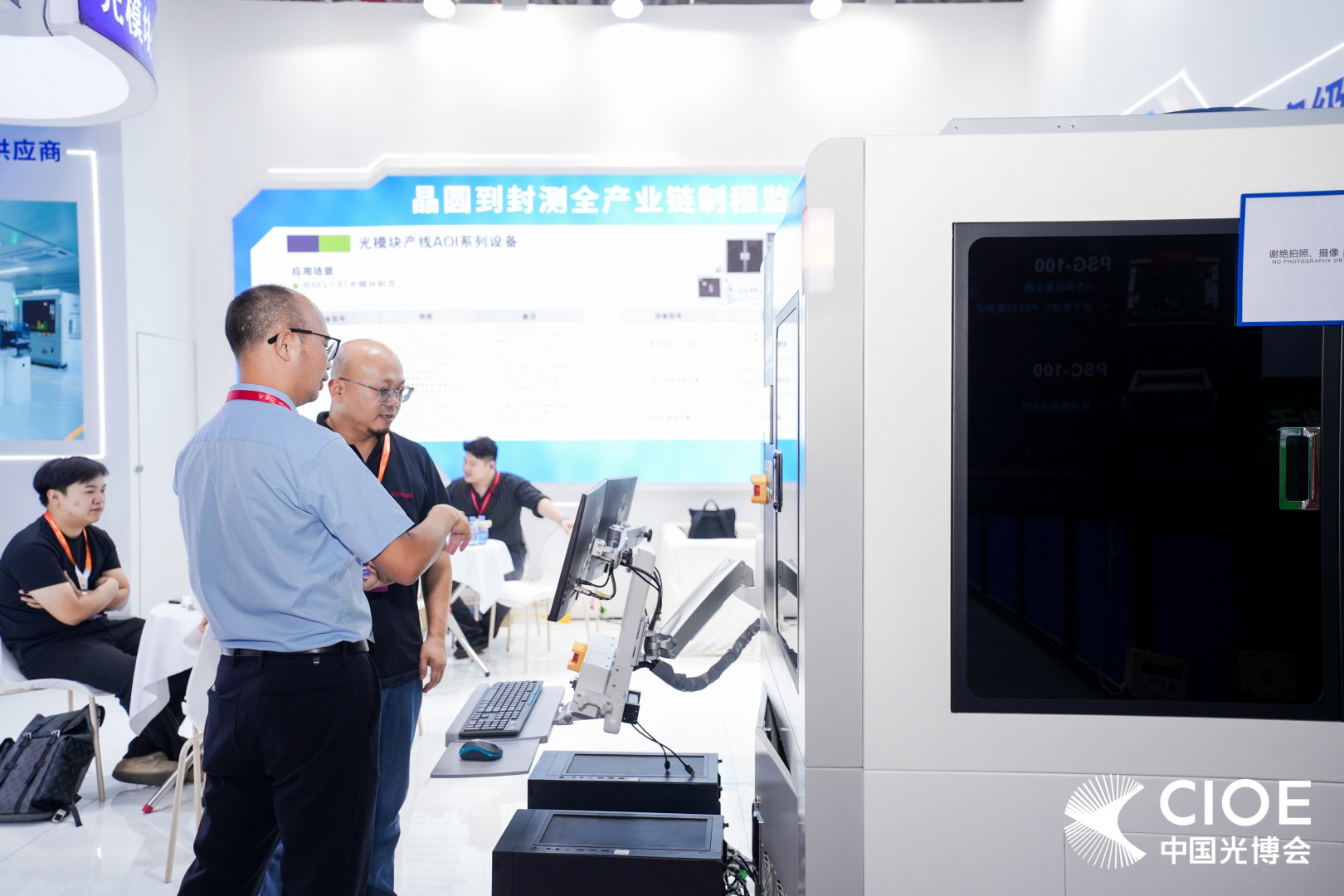
With over a decade of in-depth experience in the inspection field, Chengfeng Technology has capitalized on industry development opportunities and unveiled AOI inspection equipment specifically designed for the entire high-speed optical module manufacturing process at this year’s CIOE.
Among the showcased products, the CF915 Optical Module Gold Wire AOI Equipment is tailored for 800G/1.6T production lines, accurately identifying key defects in packaging processes such as missing gold balls, excess balls, multiple solder joints on pads, and missing dies. The CF916 DA Chip Full Inspection AOI Equipment offers comprehensive inspection of TIA/PD/PIC/COC with a maximum pixel resolution of 0.34μm. The CF917 Optical Module PCBA AOI Equipment adopts a 2D+3D inspection architecture, covering full-dimensional defect identification of components, boards, and gold fingers. The CF918 Optical Module Finished Product AOI Equipment is equipped with multiple 2D+3D camera arrays, enabling full six-sided inspection of products and identifying appearance and label defects. These four devices provide comprehensive inspection coverage from chips to substrates, from PCBAs to finished products, fortifying the quality defense line for high-speed optical module production lines.
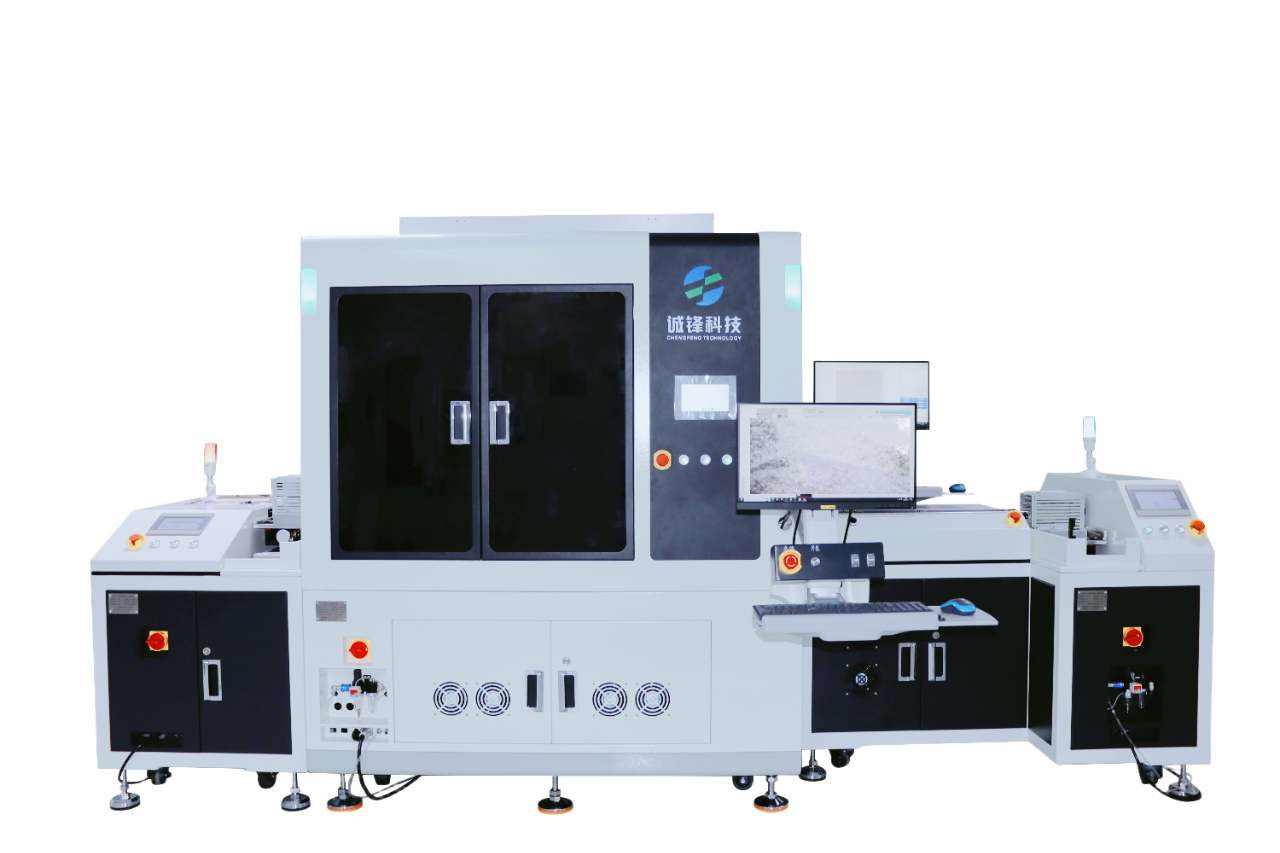
Against the backdrop of accelerated silicon photonics mass production, the CFW920 Nanoscale Patterned Wafer Defect Detection Equipment emerged as another highlight at Chengfeng Technology's booth. Designed for 800G/1.6T silicon photonics chips and advanced packaging 2D defect detection scenarios, the equipment features 10X@0.34μm and 20X@0.17μm imaging sensors, along with Die self-correction scanning capabilities and algorithms adapted to multi-color difference working conditions. It covers full industry chain process monitoring from wafers to packaging and testing.
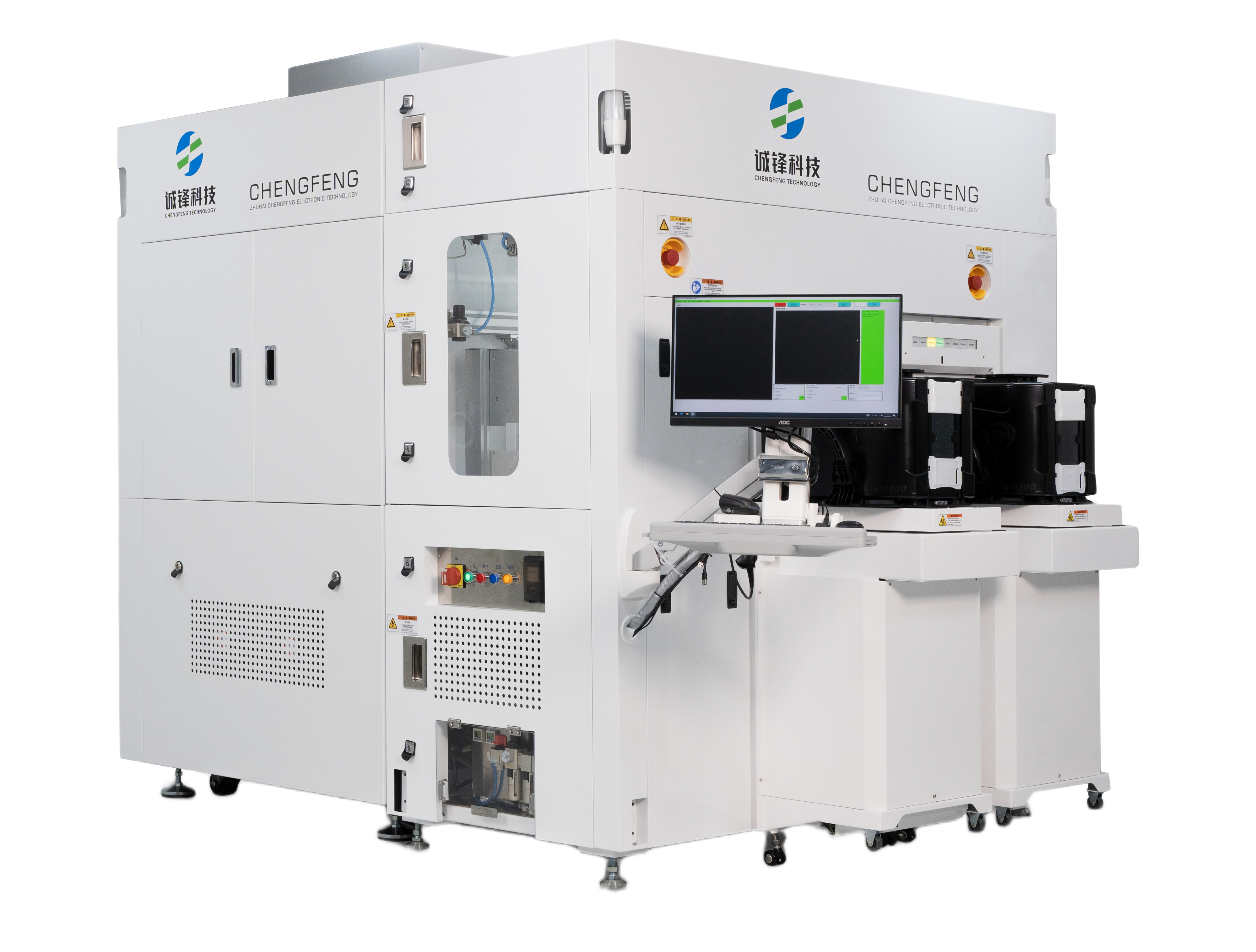
During the exhibition, Chengfeng Technology's Product Director, Ouyang Jiacheng (Owen), visited the OFweek Laser live streaming room on the afternoon of September 9. He provided an in-depth interpretation of the technological advantages of optical communication optical inspection, shared insights into the practical implementation of localized inspection equipment in the semiconductor and optical communication fields, and analyzed industry inspection pain points and solutions. This online live streaming + offline exhibition linkage format enabled industry colleagues who could not attend in person to stay updated on Chengfeng Technology's technological capabilities.
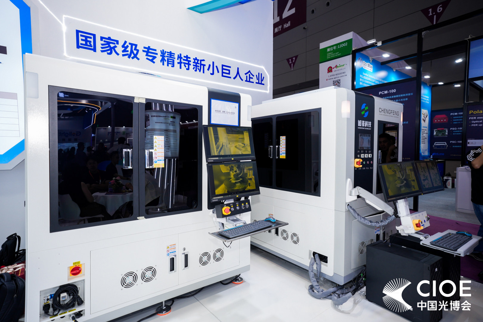
At this year's CIOE, Chengfeng Technology's booth attracted numerous professional visitors from the optical communication and semiconductor fields to stop by and exchange ideas. The technical team engaged in in-depth discussions with visiting clients on topics such as optical module process inspection, silicon photonics wafer defect identification, and advanced packaging AOI.
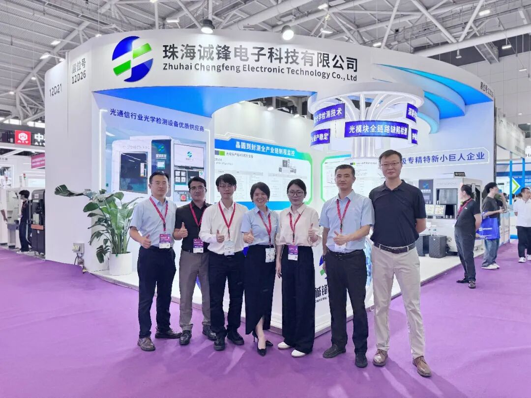
Looking ahead, as the mass production of 1.6T optical modules accelerates and CPO technology gradually moves towards commercialization, the significance of optical inspection in the optical communication industry chain will continue to grow.
Chengfeng Technology stated that the company is committed to collaborating with industry colleagues to achieve breakthroughs in the ultra-precision field of nanoscale optical inspection. It aims to make independent and controllable inspection capabilities a solid link connecting the high-quality development of the optoelectronics and semiconductor industries, jointly illuminating China's position in the AI optical interconnection era.
-
![]()
Industry-Academia Synergy! Hongshi Intelligent Partners with Tsinghua University to Overcome Key Hurdles in MicroLED Optics
-
![]()
Chengfeng Technology Shines at CIOE 2026: Bolstering the ‘Chinese Core’ of AI Optical Interconnection with Cutting-Edge Nanoscale Optical Inspection
-
![]()
Lens Revenue Rockets 42%! What’s Behind Artini Optical’s HK$13.38 Million Loss?
-
![]()
Can Seres Reclaim AITO’s Leadership? Will the ¥1.7 Billion Loss Be Reversed?
-
![]()
3 Billion Yuan: Can Neta Cars Stage a Remarkable Comeback?
-
Huawei and Seres 'Part Ways'? Seres Takes the Lead in Five Key Areas, Huawei Steps into a Supportive Role
-
![]()
Snatching Half-Yuan Electricity at Midnight, Complaining About Service Fees by Day: Who Exactly is Profiting from New Energy Charging Stations?
-
![]()
Restructuring of FAW and GAC: Not Just Merging North and South Toyota with 20 Billion Yuan