Nvidia Makes a Move, SRAM Returns to Center Stage
 03/18 2026
 553
553
Over the past two years, the global semiconductor industry's spotlight has been firmly on HBM. This DRAM, vertically stacked using Through-Silicon Via (TSV) technology, has transformed from a niche product into a highly sought-after "hard currency" alongside the large-scale shipment of Nvidia GPUs. However, in the spring of 2026, a seemingly outdated technology—SRAM (Static Random-Access Memory)—is rapidly returning to center stage.
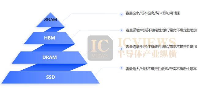
To understand the underlying logic of this resurgence, we must first clarify the basic division of labor in the memory hierarchy. In contemporary computing architectures, the memory system resembles a pyramid: at the apex is on-chip SRAM integrated near the CPU and GPU computing cores, featuring nanosecond-level access latency and highly deterministic bandwidth characteristics, albeit with extremely high bandwidth but minimal capacity and cost. Descending the pyramid are HBM, DRAM, and SSD, each level increasing in capacity but also in latency and bandwidth uncertainty. In the past, when training was the primary focus, large-capacity throughput was more critical than nanosecond-level responsiveness, hence HBM's dominance. However, as AI applications move from the lab to the masses and user experience metrics shift from "how large the model is" to "how fast the response is," the stress structure of this pyramid is undergoing profound changes.
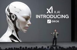
On March 17, on the stage of the SAP Center in San Jose, California, Jensen Huang, clad in his iconic black leather jacket, delivered a two-and-a-half-hour speech that formally underscored this trend. During the highly anticipated GTC 2026 keynote, Nvidia officially unveiled an inference chip integrating the Groq LPU architecture and disclosed remarkable technical details: the latest Groq 3 LPU single-chip integrates 500MB of on-chip SRAM with a storage bandwidth of up to 150TB/s, compared to the approximately 22TB/s bandwidth of mainstream GPU off-chip HBM4.
Even more striking is its rack-level solution: the Groq 3 LPX rack, equipped with 256 LPU processors, provides 128GB of on-chip SRAM and up to 40PB/s of inference acceleration bandwidth, connecting these chips through a dedicated expansion interface of 640TB/s per rack. Huang announced on-site that the chip would be manufactured by Samsung Electronics and has already entered production, with shipments expected to begin in the second half of this year. More shockingly, OpenAI has confirmed itself as the first customer for this chip, committing to invest $30 billion in procuring related inference computing power. This is not merely a technical adjustment in Nvidia's AI chip journey but a clear signal: the demand structure for AI computing is undergoing a fundamental shift, with inference replacing training as the decisive force shaping the next generation of chip architectures.
01
How SRAM is Reshaping the AI Inference Experience
To understand why SRAM is erupting at this moment, we must first clarify the historic turning point in AI workloads. Over the past five years, the central contradiction in the AI industry has been "computing power hunger"—how to stack more GPUs to build larger models. At that time, whether it was OpenAI or Google, the core appeal (demand) was to complete pre-training of massive datasets in the shortest possible time. In that phase, HBM, with its extremely high capacity and data transfer rates, perfectly served as the "granary" for GPU computing cores, despite latency issues, as throughput was the top priority.
However, Deloitte's <2026 Technology, Media, and Telecommunications Predictions> asserts that by 2026, "inference" will account for two-thirds of all AI computing capacity. As AI agents begin to undertake complex multi-step tasks and code generation tools require real-time responses to every user keystroke, the metrics for user experience have undergone a seismic shift. Users no longer care how long the model was trained; they only care about how long it takes to see the first character after asking a question (Time-to-First-Token) and whether text generation is smooth without lag (tail latency).
This is precisely the "inference split" emphasized by Groq investor Gavin Baker: the prefill stage of model processing prompts still requires the massive parallel computing power of GPUs, while the decode stage of generating responses word by word has long since shifted its bottleneck from computing power to memory bandwidth. The dilemma of traditional GPUs lies in the fact that their vast parameters are stored in off-chip HBM. For every token generated, the computing core must traverse complex packaging and interconnect lines to fetch weights from HBM. This "long-distance transport" may be tolerable during the prefill stage but causes significant latency and energy waste during the decode stage, which requires serial output of hundreds or thousands of tokens.
In large model applications, compared to relying on external HBM, SRAM can significantly reduce memory access latency and jitter for weights and activation data, thereby improving Time-to-First-Token and tail latency performance. Groq and Cerebras, two star startups, have seized this technical pain point and launched SRAM-based AI chips. When the new generation of Groq LPU boosts on-chip bandwidth to seven times that of HBM, its significance is not just numerical leadership but fundamentally altering the boundaries of the inference experience. Taking the Llama 3.3 70B model as an example, according to independent benchmarks like Artificial Analysis, the Groq platform maintains a stable inference speed of 200-300+ tokens/s across different context lengths, significantly outperforming traditional GPU inference platforms. This bandwidth determinism and latency predictability are crucial for building real-time interactive systems.
Cerebras has gone even further. According to Cerebras' official information, its Wafer-Scale Engine 3 (WSE-3) chip integrates up to 44GB of on-chip SRAM with an astonishing on-chip storage bandwidth of 21PB/s. This radical design, which turns an entire wafer into a single chip, eliminates bottlenecks in data exchange between massive computing cores and massive SRAM. In OpenAI GPT-OSS 120B inference tasks, Cerebras achieved an output speed exceeding 3000 tokens/s, approximately 15 times faster than mainstream GPU cloud inference. If Groq proves the efficiency advantage of the SRAM architecture in single-card inference, Cerebras demonstrates how close inference speed can approach its limits when SRAM capacity is sufficiently large. SRAM is like sticky notes placed on a CEO's desk—no need to wait for a secretary to retrieve files from the archives; just raise your hand to access them. This "nanosecond-level" response speed is a critical competitive advantage for building AI agents with truly real-time interactivity.
02
Nvidia's "Financial Power" and the Return of SRAM
Nvidia has clearly discerned the risks of this paradigm shift. Despite its absolute dominance in the training market, startups like Groq and Cerebras are exploiting cracks in the low-latency inference battleground with their SRAM architectures. If this trend is left unchecked, future data centers may evolve into a dual-headed pattern (landscape) of "GPUs for training, LPUs for inference," eroding Nvidia's dominant territory from the edges.
Last December, Nvidia spent $20 billion to acquire a non-exclusive license to Groq's intellectual property, including its Language Processing Unit (LPU) and accompanying software libraries, and absorbed Groq's core engineering team. The strategic significance of this deal far outweighs its financial value. It signifies Nvidia's admission that in pure serial inference scenarios, GPU architectures indeed have shortcomings, and Groq's SRAM solution is currently the best patch.
Meanwhile, the other pole of the SRAM camp is rapidly expanding. According to Cerebras' official disclosure, in February 2026, Cerebras announced the completion of a $1 billion Series H funding round, valuing it at $23 billion. More notably, OpenAI signed a $10 billion contract with Cerebras to deploy up to 750 megawatts of custom AI chips. Shortly after, in February 2026, OpenAI launched the first model running on Cerebras Systems AI accelerators—the GPT-5.3-Codex-Spark preview version, which supports code generation response speeds exceeding 1000 tokens/s, providing users with a more interactive programming experience. This series of moves clearly indicates that leading large model vendors have begun stockpiling "SRAM computing power" for the next generation of real-time interactive applications.
According to the information officially released at GTC 2026, Nvidia did not adopt a radical approach of 3D-stacking LPU units on the GPU core wafer but instead took a more pragmatic route: the Groq 3 LPU serves as an independent inference accelerator chip, combined with Rubin GPUs through a co-designed architecture to form the Vera Rubin platform. Previous analysis by Evergreen Capital pointed out that if connected via external interfaces like PCIe, data transmission would introduce new latency, partially offsetting SRAM's advantages.
This means future AI chips will feature a complex heterogeneous memory hierarchy: at the bottom are computing wafers responsible for prefill, the middle layer provides massive SRAM caches through 3D stacking for high-speed decode, and beside them, large-capacity HBM remains encapsulation (packaged) via CoWoS for storing massive contexts (KV Cache). This design retains GPU dominance in parallel computing while absorbing LPU's low-latency advantages in serial generation, all while intelligently routing different token requests through Nvidia's Dynamo inference framework and KV cache management system.
It can be said that SRAM's return is not about "killing" HBM but pushing the memory hierarchy toward a more finely divided and diversification (diversified) era.
03
Opportunities Have Arrived
Nvidia's technological shift has stirred significant ripples in the capital markets and sparked some interesting misinterpretations. When news broke that "Nvidia will launch SRAM inference chips," the Korean stock market experienced sharp fluctuations, with concerns that SRAM usage would reduce demand for HBM, impacting the core businesses of Samsung and SK Hynix. However, this fear was quickly clarified as a misjudgment by professional institutions.
From a physical standpoint, SRAM's cell area is 5 to 10 times larger than DRAM's, with extremely high cost per bit, making it impossible to replace HBM as the main memory. Even Cerebras' WSE-3, which integrates 44GB of SRAM, is an engineering marvel, but storing the full weights of a 70 billion parameter model would still require hundreds of GB of storage, which can only be handled by HBM or DRAM. SRAM's sweet spot lies in specific scenarios requiring extreme low latency, such as OpenAI's code generation tools or future physical AI robots—where every millisecond of latency could disrupt human thought flow or robotic action continuity.
In fact, the subdivision of memory layers will expand the overall market size. Every data center may now need to simultaneously equip HBM servers for training and SRAM accelerators for real-time responses. HBM handles the model's "long-term memory," while SRAM processes interactive tasks requiring "instant reactions." They are complementary, not substitutes. What Korean memory giants need to guard against is not SRAM replacing HBM but whether the proportion of GPU purchases might change with large-scale SRAM accelerator deployments, affecting HBM attachment rates.
Moreover, as the inference market's spotlight shifts to SRAM, the beneficiary logic of the semiconductor industry chain has subtly changed. Previously, HBM's prosperity primarily benefited manufacturers specializing in memory production. Now, since SRAM is directly integrated into logic chips and relies on advanced logic processes, the role of foundries has been unprecedentedly highlighted.
At GTC 2026, TSMC was explicitly named by the supply chain as "the first row of beneficiaries." As part of the embedded computing core, SRAM's design and manufacturing entirely depend on cutting-edge logic process technologies. Whether Nvidia uses the N3P process to build its next-generation LPU or AMD, Intel, and major ASIC vendors follow similar SRAM-enhanced architectures, they will ultimately rely on TSMC's advanced production lines. For TSMC, this means not only higher average selling prices per wafer (due to larger chip sizes and more advanced processes) but also solidifying its core hub status in AI semiconductor manufacturing.
Meanwhile, Taiwan's memory supply chain has found new narrative space in this trend. Previously, due to its much smaller share in standard DRAM and HBM compared to Korean vendors, it often played a supporting role in the AI storage feast. However, the rise of the SRAM route has opened a window for them. Around GTC 2026, market attention quickly focused on several Taiwanese vendors with promising prospects.
Winbond has drawn attention for its SRAM mass production experience. Its Custom Memory Solutions (CMS) business includes PSRAM (Pseudo-Static Random-Access Memory), which combines DRAM's high capacity with SRAM's high-speed interface characteristics, seen as a compromise between cost and performance. Powerchip Technology, through its 3D AI Foundry strategy, has demonstrated strength in multi-layer wafer stacking and high-capacitance interposer technologies, positioning it to undertake SRAM-related foundry work. Additionally, Etron's product line covers SRAM in 38nm and 63nm processes, with capacities aligning with Groq LPU standards; while Apacer offers next-generation ApSRAM, achieving multi-fold improvements in power consumption and bandwidth.
This indicates that while SRAM's core manufacturing lies with TSMC, related IP design, niche product supply, and advanced packaging support bring incremental opportunities for the broader domestic semiconductor ecosystem.
Looking back from this moment, SRAM's return resembles a technological samsara (cycle). In semiconductor history, every shift in computing power centers has been accompanied by memory hierarchy reconstructions. As the AI industry transitions from training frenzy to inference deep cultivation (deep cultivation), and user experience metrics shift from "how large the model is" to "how fast the response is," we are witnessing not just a product iteration by Nvidia but a generational shift. At the apex of the memory pyramid, SRAM—once shelved due to excessive costs—is now being revitalized by humanity's desire for real-time interactivity.
-
![]()
Zhao Ming Departs, IPO Postponed, AI Phones Underperform—Can Honor Still Live Up to Its Name?
-
![]()
Explosion of Recording Hardware! Four Major Product Categories Compete for New AI Entry Points, with Agent Capabilities Becoming Standard
-
![]()
China’s LEO Satellite Internet Achieves Strategic Progress: Over 100 Additional Satellites Set for Launch
-
![]()
Musk Sustains $88 Billion Loss in AI Pursuit, Now Rents GPUs to Rivals, Anticipating $500 Billion Revenue Over Three Years
-
![]()
Report | Token Economics: Envisioning a New Path for RMB Internationalization
-
![]()
Trends丨Gartner's Latest Forecast: These Seven Transformations Will Reshape the Technology Landscape Over the Next Five Years
-
Betting on Embodied AI: Bosch's New Game Plan in China
-
![]()
WeChat Collaborates with Huawei/Honor/Xiaomi on A2A: Is This the Dawn of AI Integration?