[Xijing Debut] Huawei's Tao's Law: Technical Pathways, Industry Impact, and Investment Value
 06/01 2026
 570
570

The AI race in 2026 has long moved beyond the extensive competition of 'parameter wars' in large models, with the core focus shifting to the deployment capabilities of AI agents. AI that solves real-world problems represents the true direction for creating long-term commercial value. On May 25, Huawei formally announced 'Tao's Law (τ),' marking the first time a Chinese enterprise has proposed a new principle for global industrial development in the chip sector. Herbert Zhang, a senior AI analyst at Xijing Investment, wrote about Tao's Law, analyzing its investment value from technical pathways to industrial impact.
I. Research Summary
In May 2026, Huawei published a perspective paper in Nature Electronics, proposing the Tao's Law framework, which replaces geometric linewidth with the time constant (τ, tau) as the full-stack optimization target. Through Logic Folding technology, the transistor density of next-generation chips was increased from 155 million to 238 million per square millimeter at the engineering level. The capital markets reacted strongly, with significant single-day gains in the semiconductor sector and multiple brokerage research institutions releasing in-depth reports overnight.
Based on original paper data, industrial chain research, and global benchmarking analysis, this study attempts to answer the following core questions: (1) How to evaluate the marginal returns and sustainability of logic folding technology? (2) What is the difference between the 238 million per square millimeter metric definition and industry-standard metrics? (3) Do the unit economic benefits of each segment support a closed business loop? (4) Which segments offer reasonable risk-adjusted returns at current valuation levels?
Core conclusions: Tao's Law represents a high-capital-expenditure engineering route under sanction constraints rather than a disruptive technological paradigm. The benefits of logic folding are real but exhibit diminishing marginal returns. After same-metric restoration, the true physical density is approximately 175 million per square millimeter, still representing a generational gap compared to the global leading three-nanometer process level (approximately 215 million per square millimeter). Industrial chain opportunities are concentrated in advanced packaging and hybrid bonding equipment, with most other beneficiary directions having limited relevance to the implementation of Tao's Law.
II. Technical Pathway Assessment
2.1 Engineering Positioning of the Tao's Law Framework
The theoretical core of Tao's Law is to shift the semiconductor optimization target from geometric linewidth to the time constant τ (delay), covering four levels: devices, circuits, chips, and systems. The engineering rationale for this framework lies in the fact that at nodes below seven nanometers, the intrinsic delay of transistors accounts for only 10% to 20% of the total delay, with interconnection resistance-capacitance delay (60% to 80%) and system-level data transmission delay becoming the primary bottlenecks. The advanced packaging systems of global leading foundries (such as chip-on-wafer-on-substrate packaging), three-dimensional cache stacking technology, and high-speed interconnection switching technology essentially compress system-level time constants.
From an industry perspective, the value of Tao's Law does not lie in 'inventing a new law' but in systematically integrating existing directions (advanced packaging, three-dimensional stacking, optical interconnection, unified protocols) and providing Huawei with a quantifiable performance catch-up framework under constrained process node conditions. This type of constraint-driven innovation is not without precedent in history: the Japanese automotive industry developed lean production systems after the oil crisis, and China's mobile payment sector skipped credit card stages to directly deploy QR code solutions.
 However, it must be recognized that Tao's Law represents additive optimization rather than substitutive innovation. Global leaders, while possessing extreme ultraviolet lithography (EUV) advanced processes, are also advancing three-dimensional stacking and advanced packaging. The same stacking optimizations yield far greater marginal returns when applied to two-nanometer nodes than to seven-nanometer nodes. This is not 'bending the curve' but catching up on the straightaway at a higher comprehensive cost (design complexity, capital expenditure, thermal management solutions).
2.2 Marginal Return Analysis of Logic Folding
The engineering implementation path of logic folding involves distributing logic gates (gate-level circuits and flip-flops) on critical paths across two active silicon layers, achieving vertical interconnection through 1.5-micron-spaced hybrid bonding (Hybrid Bonding), thereby shortening the wiring length of critical paths. Key parameters disclosed in the paper include: hybrid bonding spacing of 1.5 microns, overlay accuracy below 0.5 microns, through-silicon via (TSV) critical dimensions and isolation regions smaller than 1.5 microns, TSV spacing less than 6 microns, and a spacing ratio (hybrid bonding spacing to top-layer metal spacing) of approximately 2. 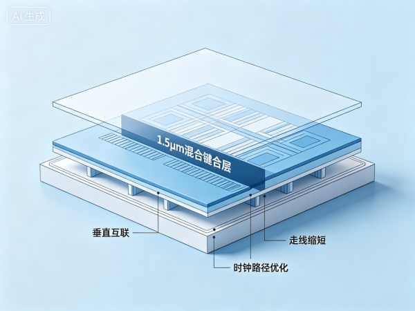
In terms of performance improvement, the benefits of logic folding are real and derivable: a 42% reduction in clock tree depth stems from vertical reconstruction of the clock tree, a 28% reduction in clock wire length and a 25% reduction in clock skew stem from shortened horizontal wiring, and a 30% reduction in static random-access memory (SRAM) delay stems from shortened bitlines and wordlines. These improvements all result from topological optimization rather than enhancements in intrinsic transistor performance. The clock frequency increase from 2.75 gigahertz to 3.1 gigahertz (a 12.7% improvement) aligns with physical expectations from timing margin release.
Diminishing marginal returns represent the core constraint of the logic folding pathway. The first generation, moving from single-layer to double-layer folding (covering approximately 53% of chip area through selective folding), achieves a density increase of approximately 53.5%. If advanced to full-chip folding (expected by 2030), the density increase would be approximately 88%. Moving from double-layer to triple-layer folding (expected by 2031) would yield an incremental benefit of approximately 50%; from triple-layer to quadruple-layer, the incremental benefit would further decline to 33%. Meanwhile, each additional layer non-linearly increases thermal management complexity, EDA toolchain requirements, and manufacturing costs.
III. Metric Calibration and Data Restoration
When conducting cross-company benchmarking, the primary task is to ensure consistent metric definitions. The density data of 155 to 238 million per square millimeter in the Tao's Law paper involves at least two layers of metric differences requiring calibration:
First layer: Formula coefficient differences. The paper uses Huawei's formula (coefficient 2.0) for density calculation, while the prevailing formula (Boyle's metric) has a coefficient of 1.474. The ratio between the two is 1.357 times, explaining why density figures for the same process, same foundry, and same time point differ by over 30%.
Second layer: Three-dimensional projection merged calculation. The 238 million per square millimeter figure does not represent the planar process density of a single silicon layer but rather the effective density obtained by merging transistor counts from both active logic layers (upper and lower) based on top-view projected area. Specifically, three-dimensional density equals (lower-layer transistor count plus upper-layer transistor count) divided by projected area, where the numerator increases while the denominator remains constant.
After calibrating formula coefficient differences, the actual physical level of the new-generation chip falls between globally leading five-nanometer and three-nanometer processes, consistent with its technical reality as a seven-nanometer-class process under current process node constraints. The critical recognition is that equivalent density cannot be directly equated with performance. Transistor density is merely one variable in the performance equation, with intrinsic speed, leakage current control, power efficiency, and other parameters being equally important in advanced process competition—parameters that can hardly be compensated for through three-dimensional stacking.
IV. Unit Economic Benefits and Hidden Costs
When evaluating technical routes, unit economic benefits must be dissected. The cost structure of the logic folding route can be broken down into the following modules:
Chip costs: Traditional single-die solutions involve one wafer cost plus one mask set plus one tape-out. The logic folding solution involves two wafer costs (two independent lithography layers) plus two mask sets (with partial mask reuse possible) plus two tape-outs plus bonding process costs. The bonding process includes: chemical mechanical polishing (surface flatness < 1 nanometer), cleaning (particles < 0.1 micron), alignment (overlay accuracy < 0.5 micron), and annealing. Hybrid bonding equipment costs approximately $5 million to $8 million per unit, with throughput of about 30 to 60 wafers per hour, requiring depreciation to be allocated to each chip.
Yield impact: The overall yield of three-dimensional stacking equals the yield of the lower chip multiplied by the yield of the upper chip multiplied by the bonding yield multiplied by the TSV yield. If single-layer yield is 90%, bonding yield is 95%, and TSV yield is 99.9%, the overall yield would be approximately 77%—far lower than the 90% of traditional single-die solutions. The paper claims that intelligent redundancy and repair architectures can elevate functional yield to nearly 100%, but this also means requiring additional redundant circuit area.
Thermal management solution costs: Logic layer stacking increases power density by approximately 40% (after accounting for a 41% energy efficiency improvement). The first-generation solution (53% selective folding) requires MEMS microfans ($2–$3 per unit) plus micro-pump liquid cooling channels (adding packaging process steps). If advanced to full-chip folding or triple-layer stacking, thermal management solutions would need upgrading to diamond heat dissipation layers plus fluorinated liquid microchannels, potentially increasing thermal material costs to $5–$8 per unit.
EDA tool and design costs: Existing EDA toolchains do not support native three-dimensional design. The paper acknowledges that scaling (scaled) logic folding requires 'a completely new three-dimensional native toolchain,' including cell-level partitioning, cross-chip timing convergence, and wafer-level process variation modeling. This implies: (1) significant increases in one-time engineering costs for self-developed or heavily customized design tools; (2) extended design cycles and increased uncertainty in time-to-market; (3) severe talent shortages, with extremely limited supply of engineers experienced in relevant design work. 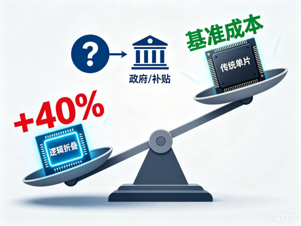
Comprehensive assessment indicates that the total cost of ownership for the logic folding route is expected to exceed that of traditional single-die solutions by over 40%, explaining why terminal chip manufacturers with advanced processes would not adopt similar approaches. Dependence on government subsidies (equipment procurement subsidies, tape-out subsidies) represents a core variable for the long-term sustainability of this route.
V. Industrial Chain Value Assessment
Based on the above analysis of unit economic benefits and hidden costs, we qualitatively assess the certainty, competitive landscape, valuation levels, and potential returns of each segment:
Segment
Certainty
Competitive Landscape
Valuation Level
Priority
Advanced Packaging
High
Good
Reasonable
Priority
Hybrid Bonding Equipment
Medium-High
Excellent
High
Priority
Testing Equipment
Medium
Good
Reasonable
Secondary
Liquid Cooling
Medium
Average
High
Secondary
Design Automation Tools
Low
Average
High
Observe
Table: Attractiveness Matrix of Industrial Chain Segments
Logic underlying directional judgments:
(1) Advanced packaging represents the core enabling segment for Tao's Law implementation, with the highest certainty and verifiable capacity ramp-up rhythm (pace); (2) Hybrid bonding equipment constitutes the most critical segment for equipment localization logic, with significant market potential if domestic manufacturers pass customer verification; (3) Thermal management solutions have broad applicability, but attention should be paid to frontier innovation solutions such as micro-pump liquid cooling, MEMS fans, and diamond heat dissipation; (4) Testing equipment represents a silent beneficiary, with three-dimensional chip testing unit prices and durations significantly exceeding those of two-dimensional chips.
Key insights:
(1) In the advanced packaging segment, competition among domestic OSAT companies centers not on 'who can do it' but on 'who can secure capacity allocation,' with Huawei-affiliated incubator companies enjoying priority in advanced packaging capacity allocation. (2) In the hybrid bonding equipment segment, overseas leaders still maintain generational advantages in precision control (overlay accuracy, throughput), with domestic substitution representing a gradual rather than abrupt process; focus on bonding equipment companies with actual mass production delivery. (3) The thermal management segment faces the most intense competition, with technology routes yet to converge (MEMS microfans/microchannels/diamond thermal conduction), and leadership positions established on commercialization first-mover advantages rather than technological barriers.
VI. Directional Judgments
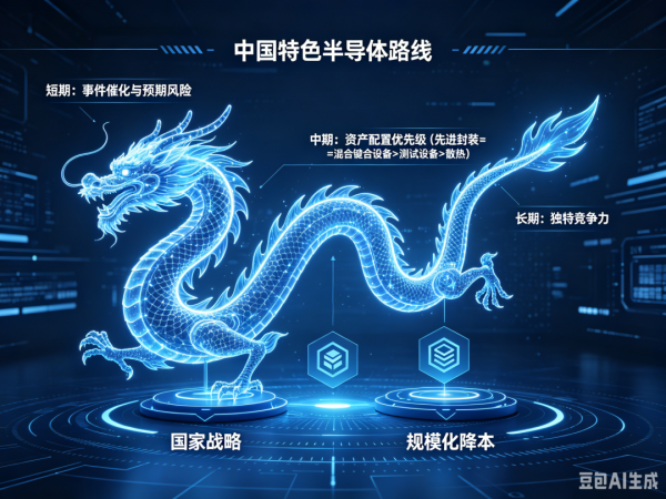
Current market sentiment stands at elevated levels, with dense (intense) event catalysis (paper publication, media promotion, policy signals) overlapping with interim report expectations, creating risk of expectation overhang in the sector in the short term. In the medium term, under Tao's Law, asset allocation priorities are: advanced packaging = hybrid bonding equipment > testing equipment > thermal management. From a longer investment horizon, the true value of Tao's Law lies not in catching up with advanced processes but in validating the feasibility of a Chinese-characteristic semiconductor roadmap: using high-cost advanced packaging solutions to compensate for process gaps and achieve acceptable performance in end products. Supported by national strategy, if this roadmap can achieve continuous cost reductions through scaled applications, it may develop unique competitiveness in advanced packaging.
-
Ofilm Teams Up with ADSensE to Propel Large-Scale Deployment of All-Solid-State LiDAR Powered by ADS6311 Chip!
-
![]()
Loss of 2.5 Billion Yet Facing Strong Demand for Shares? Another Battle for Control of Lianchuang Electronics
-
![]()
Huawei’s Enjoy Series Flies Off the Shelves, Prompting Xiaomi to Double Down on Budget Smartphones
-
![]()
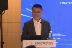
Beijing Hyundai's Top Executive Criticizes Industry Disorder: Certain Brands Treat Customers as Beta Testers
-
![]()
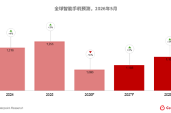
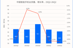
The domestic mobile phone market has declined for five consecutive quarters! Huawei defies the trend with significant growth: maintains its top market share
-
Annual Revenue Surpasses 3 Billion: An Automotive Trim 'Little Giant' Makes Its Debut on the Beijing Stock Exchange
-
![]()
The Space Force Wants to Spend $30 Billion on Rocket Launches: Is Trump Doubling Down, and Is SpaceX the Big Winner?
-
![]()
Going Crazy! One out of Every Three Plug-in Hybrids Sold in Europe is a Chinese Vehicle