Why Did Tesla Award Samsung Electronics a $16.5 Billion Chip Order?
 08/04 2025
 752
752
Produced by Zhineng Zhixin
Tesla and Samsung Electronics have inked a long-term $16.5 billion chip foundry agreement. This deal marks Samsung's reclaiming of a key customer in advanced manufacturing, while Tesla, with its ambitions in autonomous driving and humanoid robotics, strategically relies on high-performance AI chips.
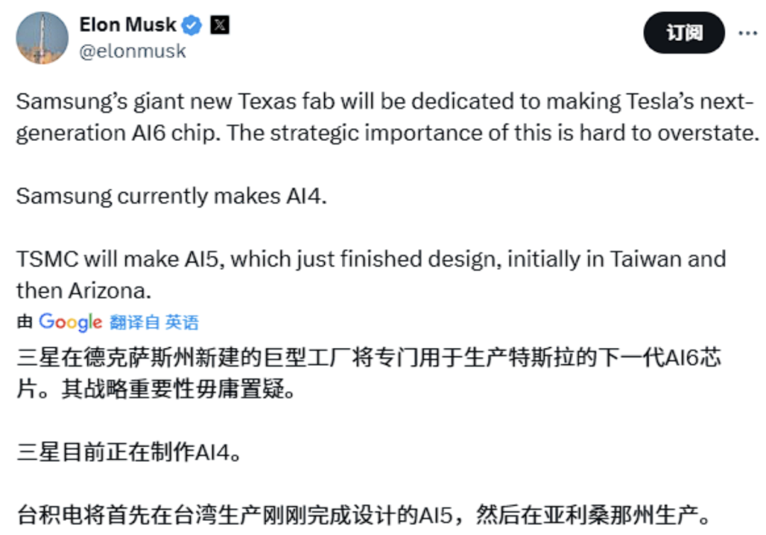
At the heart of this partnership lies the upcoming AI6 chip, set to be manufactured at Samsung's Texas plant and destined to become a vital component in Tesla's Full Self-Driving (FSD) system. In the fiercely competitive realm of AI chip foundry services, this collaboration signifies a profound technological synergy for both entities.
Part 1: Tesla's AI Chip Evolution and Foundry Distribution
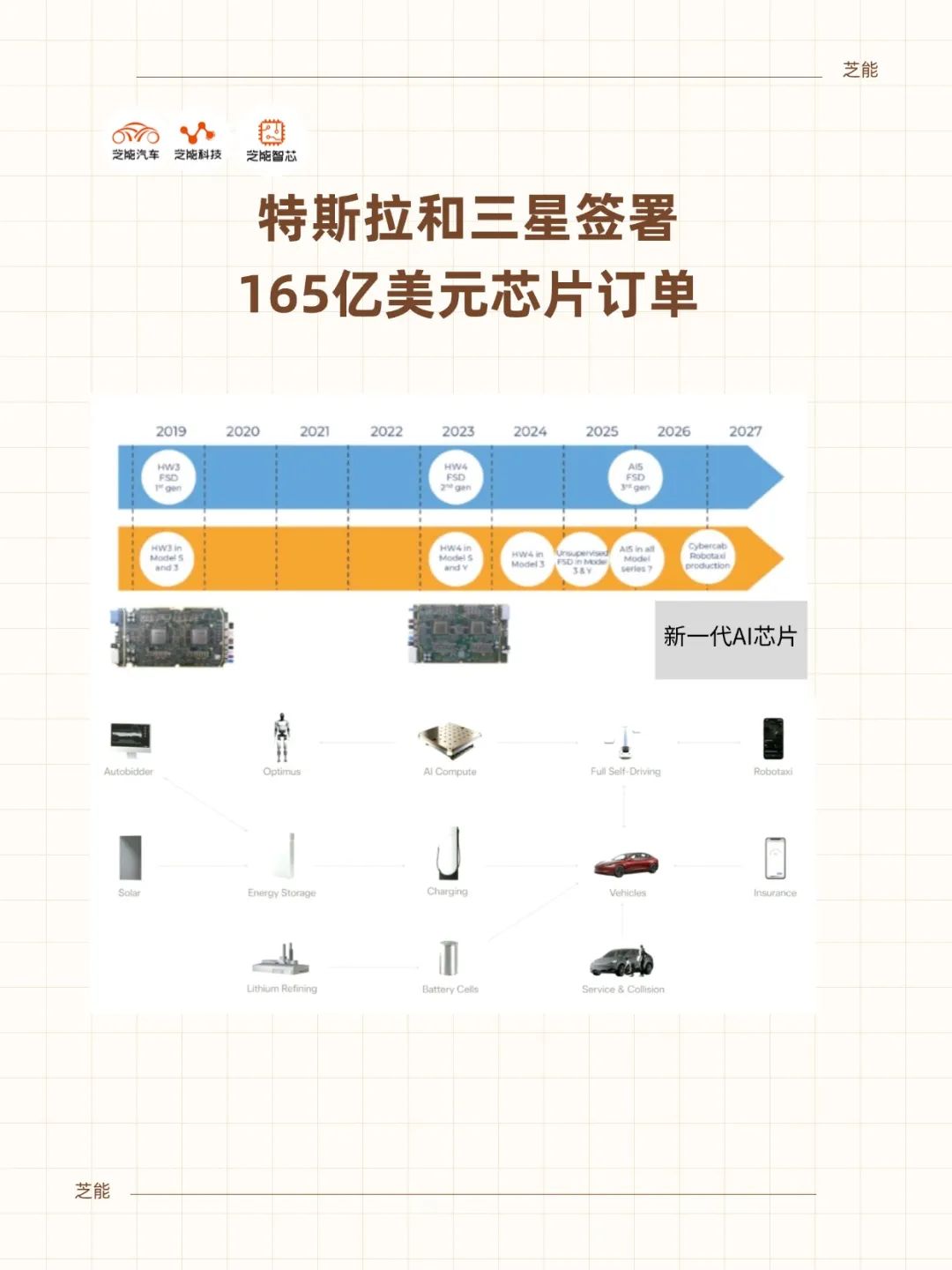
The focal point of this collaboration is Tesla's sixth-generation AI chip, the "AI6," anticipated to be integrated into autonomous driving systems and humanoid robot platforms set for mass production in the coming years. Drawing from public information, Tesla employs a "hybrid foundry" model for the design and production of its AI chips, with different fabs handling different iterations.
Previously, Samsung manufactured the AI4, while TSMC handled the AI5. The AI6's return to Samsung underscores that, at specific manufacturing nodes and packaging solutions, Samsung aligns with Tesla's comprehensive requirements for performance, timelines, and collaborative capabilities.
The core design of AI chips typically encompasses modules such as large-scale matrix multiplication acceleration units (Transformers), neural network-specific execution engines, on-chip high-bandwidth caches (SRAM), and high-speed I/O interfaces (like PCIe Gen5/6 or NVLink).
Building on past experience, Tesla's FSD chips leverage a proprietary AI SoC architecture, with a roadmap centered on high-throughput neural network inference capabilities, prioritizing low-latency real-time performance and system redundancy.
From a manufacturing standpoint, the AI4 likely utilized a 7nm FinFET process, while the AI5 advanced to a 5nm process. The AI6 is poised to enter the 3nm GAA (Gate-All-Around) era, and Samsung's receipt of this order signifies a significant validation of its second-generation 3nm process, SF3 (based on MBCFET structure).
In contrast to TSMC's current stable mass production of N3B and upcoming N3E, Samsung's SF3 technology path carries higher risks and started later, but it theoretically offers superior density and power consumption control.
For the AI6 chip, the AI computing units demand significant size and power consumption, necessitating fabs equipped with advanced EUV lithography, stacked packaging (such as 2.5D/3D packaging), and yield control capabilities.
Samsung, with years of experience in EUV processing and high-performance logic manufacturing, has tasked its new plant in Taylor, Texas, with producing the AI6, marking the plant's first major commercialization validation.
Part 2: Samsung Chip Foundry: Technological Gamble and Capacity Breakthrough
Samsung holds a "dual identity" in the global chip manufacturing industry: it is both the world's largest memory chip maker and the second-largest wafer foundry.
Despite its vertical integration advantages, Samsung has consistently been overshadowed by TSMC in the foundry market. In the first quarter of 2024, its global foundry market share stood at only 7.7%, paltry in comparison to TSMC's 67.6%.
The gap is not solely attributable to technical capability but rather a combination of systematic strengths such as comprehensive ecosystems, customer trust, production line stability, and IP support. For an extended period, Samsung has grappled with a vicious cycle of "underutilized capacity - financial losses - lack of customer confidence," and the construction timeline and production ramp-up of its Texas plant were once delayed until 2026.
AI chip foundry services present a potential turning point for Samsung.
AI chips are typically characterized by large order volumes, high technical barriers, and long lifecycles. Once customer trust is established, they have the potential to span multiple iteration cycles. Tesla's AI6 chip will be produced continuously until 2033, providing Samsung with a stable order platform for nearly a decade.
Furthermore, Musk has clarified that Tesla will actively participate in optimizing the manufacturing process, signifying that customers will not only procure but also deeply collaborate in design, validation, packaging, and testing, fostering the continuous improvement of Samsung's foundry processes.
Technologically, Samsung's 3nm GAA process employs the MBCFET (Multi-Bridge Channel Field Effect Transistor) architecture, which theoretically significantly reduces short-channel effects and enhances transistor switching efficiency and power consumption ratio. However, the challenges of the GAA architecture lie in increased manufacturing complexity and higher requirements for EUV lithography equipment control precision, deposition processes, and consistency management.
Samsung already has customer tape-outs at the SF3 node, but capacity has yet to ramp up. The large-scale introduction of the AI6 is expected to be a pivotal inflection point for the maturity of its GAA process.
Moreover, the Tesla order will propel Samsung's investment in advanced packaging (such as FOWLP or H-Cube 3D packaging) to meet the integration and thermal management demands of AI SoCs.
In terms of competition, Samsung faces not only TSMC. The HBM (High Bandwidth Memory) field is dominated by SK Hynix, and TSMC excels in CoWoS packaging and HBM integration. Future AI SoC foundry services are no longer straightforward logic process competitions but comprehensive battles encompassing front-end manufacturing, advanced packaging, package memory integration, and system debugging.
Summary
The collaboration between Tesla and Samsung underscores that AI chip foundry services have evolved beyond mere single-customer procurements to the construction of a highly collaborative and long-term industrial community. Tesla views AI chips as the cornerstone of its robot and autonomous driving strategies, while Samsung sees this as an anchor point for the revitalization of its foundry business.
The rollout of the AI6 chip will validate Samsung's capabilities across multiple dimensions, including the 3nm GAA process, capacity scheduling, quality control, and advanced packaging, laying the groundwork for attracting other AI chip customers, including startups and fabless companies.
-
![]()
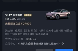
Discounts Now on Offer: Is Xiaomi No Longer Grappling with Vehicle Shortages?
-
![]()
Samsung Doesn't Make Money the Hard Way
-
![]()
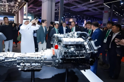
Japanese Media Acknowledges: China's Engine Technology Outstrips That of Japanese Firms
-
![]()
Japanese Media Concedes: China’s Engine Technology Outpaces Japanese Firms
-
![]()
Doubao Professional Version Unveiled! China Now Boasts Its Own National-Level Professional AI Agent
-
![]()
ByteDance and Alibaba Both Step Back from the Gaming Arena
-
Xiangeo International Clears BSE Review: Setting a Global Standard for the ‘Chinese Sound’ | A-Share Financing Brief
-
![]()
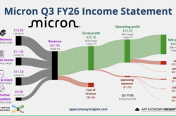
86% Gross Margin, Revenue Hits 48-Year High: Micron Warns of Prolonged Supply Tightness Beyond 2027