From HW1.0 to AI5: Has Tesla's Chip Seen a Radical Transformation?
 06/03 2026
 540
540
Back in 2014, the first-generation Autopilot hardware, Mobileye EyeQ3, boasted a computing power of 25TOPS. Fast forward a decade, and Tesla's next-gen FSD computing platform, AI5, has skyrocketed to an impressive 2000-2500TOPS. This leap in performance isn't just about cramming more transistors onto a chip; it's a fundamental rethinking of chip design philosophy. In June 2024, Elon Musk took to social media to announce that the fifth-gen in-vehicle computing platform, initially dubbed HW5.0, would now be known as AI5. By June 2025, AI5 had officially entered mass production, with TSMC and Samsung as its co-foundries.
HW4.0, built on Samsung's 7nm process, delivered a computing power range of 300 to 500 TOPS. In stark contrast, AI5 jumps straight to TSMC's cutting-edge 3nm N3P process, with Samsung stepping in as a backup foundry—a role that's only expected to kick in when mass production of AI5-equipped vehicles starts in 2026. The result? A five- to eightfold increase in computing power and a staggering fortyfold improvement in performance. This isn't just a process node transition; it's a game-changer. What's really shaking up the industry, though, is Tesla's unconventional approach to chip design: subtraction.

AI5: Ditching Traditional GPU and ISP Image Signal Processors?
When most chip companies design their products, they aim to cover as many bases as possible. Take NVIDIA's GPUs, for instance; they're built to handle gaming, rendering, scientific computing, autonomous driving, and more. That means keeping a bunch of general-purpose modules on board. Tesla, however, marches to the beat of its own drum. AI5 is designed for one client and one client only: Tesla itself. So, the architects made a bold move: they stripped the GPU and ISP right out of the chip.
What does that mean? Well, graphics rendering tasks are now entirely offloaded to the cockpit chip (an AMD Ryzen processor). The FSD chip can focus solely on neural network inference without getting distracted by screen display duties. And the ISP, which traditionally processes raw sensor data into visually pleasing images by reducing noise, adjusting colors, and sharpening, is bypassed. Why? Because for neural networks, these processes are just a form of filtering that loses raw information. AI5 feeds raw 12-bit photon data directly to the neural network, resulting in cleaner data, lower latency, and minimal information loss.
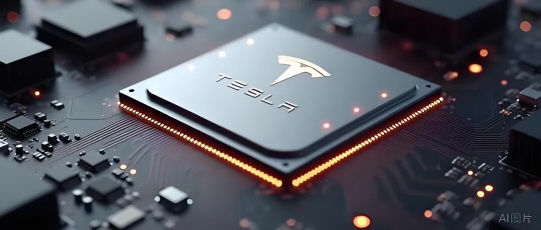
Image Source: Internet
This subtraction strategy allows the chip's area to fit neatly within one and a half photomasks. In semiconductor manufacturing, a photomask is the foundation for lithography—the bigger the mask, the lower the yield. AI5's area is precisely within the upper limit of one and a half photomasks, enabling the entire chip to be fabricated in a single exposure without stitching multiple masks together. This not only cuts manufacturing costs but also boosts the number of chips per wafer and reduces defect rates. The saved transistor budget can then be entirely devoted to AI inference-specific computing units.
But hardware-level streamlining is just part of the story. AI5 also gets customized upgrades at the instruction set level. Take SoftMax, a common neural network operation that converts numerical values into a probability distribution. Running this on AI4 required simulating forty steps with conventional instructions. AI5, on the other hand, natively supports this instruction at the hardware level, completing it in just a few steps. Saving over thirty steps per operation, multiplied by the millions or even billions of times it's invoked in a neural network, amplifies the performance gap by several dozen times. That's why, despite AI5's raw computing power being only five to eight times higher than AI4, its actual inference performance can reach fortyfold or even greater improvements.

Are Sensor Configurations Changing Too?
Reports suggest that in the AI5 hardware suite, Tesla has upped the camera count from nine to twelve, upgrading their resolution from 5 megapixels to 8 megapixels. These aren't just simple lens swaps; the new modules come with integrated lens heating elements to quickly melt ice in snowy conditions and hydrophobic coatings to reduce water adhesion. Winter drivers in northern regions will surely appreciate this upgrade. Traditional cameras become useless when fogged or iced over, rendering the perception system ineffective. Tesla, well aware of this Achilles' heel in pure vision systems, has opted for a hardware solution.
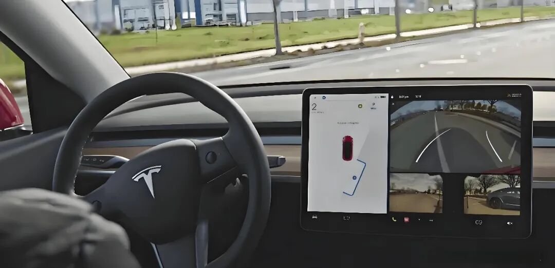
Image Source: Internet
Moreover, Tesla has reintroduced four 4D millimeter-wave radars in AI5. These radars not only measure distance, speed, and azimuth but also altitude, and they're unaffected by rain, snow, or fog. Paired with twelve high-definition cameras, the perception system forms a complete multi-modal redundancy framework at the hardware level. However, in AI5, backend decision-making remains an end-to-end pure neural network. Data from all sensors converges into a single inference pipeline, with a unified model making the final driving decisions.

What Can 2500 TOPS of Computing Power Do?
As mentioned earlier, AI5 delivers a whopping 2000-2500TOPS of computing power per chip. For comparison, NVIDIA's Thor-X chip offers around 2000TOPS, while NIO's Shenji NX9031 exceeds 1000TOPS. Clearly, AI5's single-chip performance is highly competitive.
But it's not just about raw computing power; the memory subsystem has also been upgraded. AI4 used GDDR6 video memory with a bandwidth of approximately 384 GB/s. AI5, on the other hand, features twelve SK Hynix LPDDR5X memory chips surrounding the chip, each with a capacity of 16GB, for a total capacity ranging from 144GB to 192GB. Based on a 384-bit memory interface, bandwidth is conservatively estimated at around 900GB/s and could potentially exceed 1.5TB/s under optimistic estimates.
Given the extremely high cost of HBM, which requires silicon interposer packaging and longer automotive-grade certification cycles, Tesla opted not to use the HBM3 solution but instead chose the mature LPDDR5X path. Memory bandwidth is crucial for ensuring the chip can fully utilize its computing power when running large models without idling due to insufficient data feed. AI5's 900GB/s-class bandwidth represents a roughly 2.3-fold improvement over HW4's 384GB/s, sufficient to support real-time inference of large models with hundreds of billions of parameters.
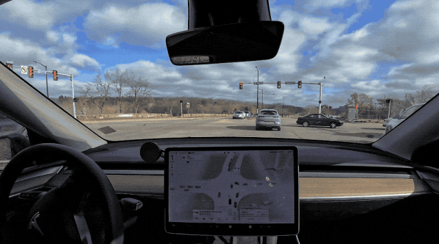
Image Source: Internet
AI5's energy efficiency is also remarkable. At a peak computing power of 2000TOPS, its power consumption is approximately 200W—about one-third of NVIDIA's Thor-X at the same computing power level. Its energy efficiency ratio ranges between 810TOPS/W and 10TOPS/W. Low power consumption significantly reduces the burden on the vehicle's cooling system, allowing more battery energy to be allocated to propulsion.
One key reason for AI5's energy efficiency improvements is Tesla's support for INT8 and INT4 quantization. Traditional floating-point operations are computationally complex and power-hungry, whereas integer operations utilize logic gates that are nearly half as simple, reducing power consumption by over 60% and latency by threefold for the same tasks. Tesla employed quantization-aware training (QAT) during model training, achieving substantial power consumption reductions at the chip level while controlling accuracy loss to less than 1%.
Another technical detail of AI5 lies in its memory configuration. Reports suggest it's equipped with 144GB of LPDDR5X memory, deeply optimized for the Transformer architecture, capable of simultaneously processing real-time footage from twelve high-definition cameras and multiple trajectory predictions. In contrast, AI4's memory configuration was around 16GB, which gradually became inadequate when handling more complex long-tail scenarios such as unprotected left turns and dense construction zones. The increased memory capacity allows AI5 to run significantly larger end-to-end neural network models. With the current FSD model's parameter scale continuously growing, the hardware's memory limitations must be addressed proactively.

Will AI5 Take FSD from Good to Great?
In December 2025, a Model 3 set off from Los Angeles, traveling eastward and covering 4,397 kilometers across the United States in 2 days and 20 hours without any human intervention. In May 2026, a group of Tesla owners completed a cross-Canada autonomous driving test, starting from Vancouver and covering 3,760 miles (approximately 6,051 kilometers) in 4 days and 21 hours, also without any human intervention.
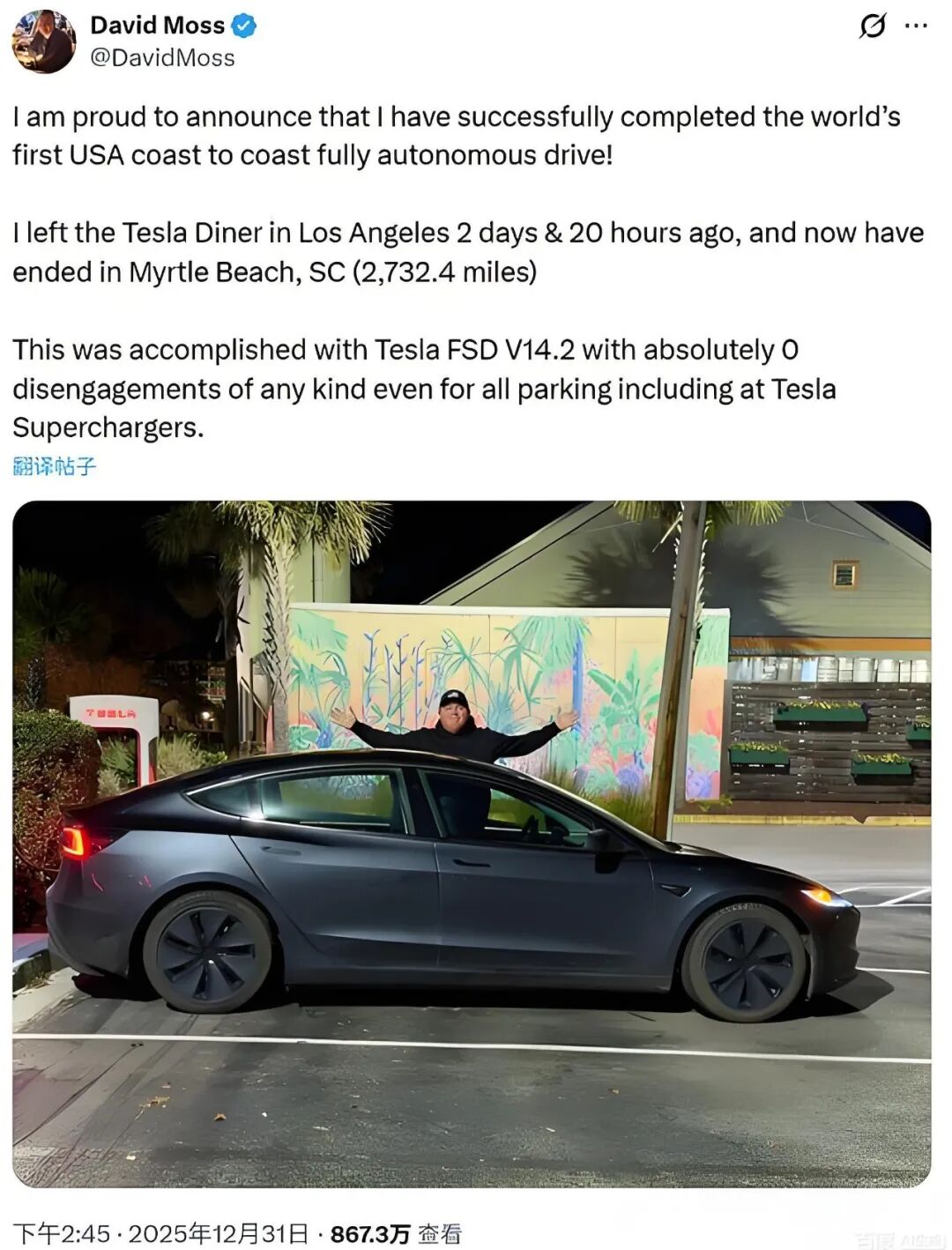
Image Source: Internet
These real-world tests demonstrated FSD's ability to operate continuously under complex road conditions. Despite encountering heavy rain, construction zones, and nighttime driving, the system didn't relinquish control due to scenarios exceeding preset rules but instead automatically completed the entire driving process. Behind this system runs an end-to-end neural network architecture.
FSD V12 has removed over 400,000 lines of C++ rule-based code, directly outputting control signals for steering, acceleration, and braking from the camera's raw data. All decision-making logic is entrusted to the neural network for self-learning. Running such a model requires exceptionally powerful hardware, as end-to-end models demand exponentially higher computing power than traditional modular architectures. AI5's high computing power, high bandwidth, and native SoftMax acceleration are precisely tailored for this unified large model architecture.

Leading in Energy Efficiency and Lower Costs?
From a cost perspective, AI5 is highly competitive. Elon Musk publicly stated that AI5's cost is merely one-tenth of NVIDIA's equivalent chip. This cost reduction is achieved not only by eliminating numerous general-purpose modules through a specialized architecture, reducing chip area, and improving wafer utilization but also by leveraging the bargaining power derived from a dual-foundry strategy. TSMC handles the primary mass production, while Samsung serves as a backup. With two factories vying for orders, costs naturally decline. This A-primary, B-backup model is rare in the automotive chip industry. While most automakers struggle with delivery schedules for a single Orin X chip, Tesla is already establishing a dual-supply chain.
In terms of process node selection, AI5 also showcases flexibility. TSMC employs its 3nm N3P process as the mainstay, while Samsung plans to use a 2nm process for trial production. Both factories are located in the United States—in Arizona and Texas, respectively—reducing supply chain risks to a relatively low level.

Delayed Mass Production: How Long Will Cybertruck and Robotaxi Wait?
Based on currently disclosed data, AI5's hardware configuration is indeed impressive. However, uncertainty remains regarding when this system will truly be integrated into vehicles. In June 2024, Musk announced that AI5 would be installed in vehicles in the second half of 2025. Yet, by the end of 2025, mass production was pushed back to mid-2027. According to the most optimistic estimates, engineering samples and small-batch trial production of AI5 might emerge by the end of 2026. However, reserving several hundred thousand AI5 motherboards is necessary to switch over entire vehicle production lines. This implies that the Cybercab and Robotaxi models originally scheduled for mass production in 2026 will likely still use AI4 hardware.
Image Source: Internet
To fill the gap caused by AI5's delayed mass production, Tesla temporarily introduced AI4.5 as a transitional solution for the 2026 Model Y. Nevertheless, Musk has made a long-term commitment: starting with AI6, Tesla will compress its chip design cycle to nine months per generation. This claim has sparked considerable discussion within the semiconductor industry, as even Apple maintains an annual chip update rhythm. However, Tesla's logic is that its chip design serves only one client, resulting in a shorter iteration chain than any general-purpose chip company. If this rhythm proves viable, Tesla's leading advantage in automotive AI chips will further widen.

The Final Word
Over the span of eleven years, Tesla has advanced from HW1 to AI5, witnessing an explosive increase in computing power from a mere 0.256 to a staggering 2500—a growth trajectory that defies the conventional pace of iterative development. However, computing power alone is not the ultimate objective. AI5 actually offers a solution to a pivotal question: as autonomous driving shifts from a rule-based paradigm to a large model-driven era, what form should an in-vehicle computing platform take? The answer does not lie in simply piling on more transistors or stuffing in redundant modules. Rather, it entails a radical simplification focused on a singular task—channeling all transistors towards a unified objective, allowing software and hardware to evolve in tandem under a cohesive logic.
-- END --
-
![]()
From 'Hardware Price Comparison' to 'Endurance Race': Who Will Lead the Heavy-Duty Truck Sector?
-
![]()
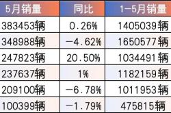
Sales of Six Major Chinese Automakers in May: BYD Reclaims Top Spot, Domestic Market Under Pressure While Exports Drive Growth | Mirror Pro
-
![]()
Search Will Enter the Third Phase of Its Lifecycle: Search as Code
-
![]()
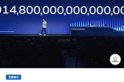
Computex 2026 | Qualcomm’s Visionary Outlook: In the Age of Agents, Devices Take Center Stage in Computing
-
![]()
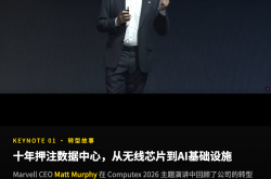
Computex 2026 | Marvell: How to Connect Data Centers in the AI Era?
-
![]()
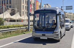
【Intelligent】Tianjin Launches Its First L4 Autonomous Bus Route
-
![]()
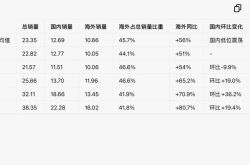
BYD’s Monthly Overseas Sales Soar Past 160,000 Units: Elevated Gross Margins Drive Profitability!
-
![]()
Tencent's Trump Card Has Never Been Large Models