Where is the AI Infra Industry Chain Bottlenecked?
 04/24 2026
 662
662
As phenomenal AI applications like DeepSeek and Seedance 2.0 continue to roll out, global demand for computing power is surging far beyond expectations. However, behind the computing arms race, the AI infrastructure (AI Infra) industry chain is encountering unprecedented systemic bottlenecks. From core equipment in chip manufacturing to a single copper cable in data centers, from specialty materials to cleanroom facilities, nearly every critical link has hit a "red light."
01
The Four "Walls" of Computing Power Development
The development of AI computing power is not merely about improving chip performance in a single dimension but rather a complex systems engineering project involving computing, storage, transmission, and energy.
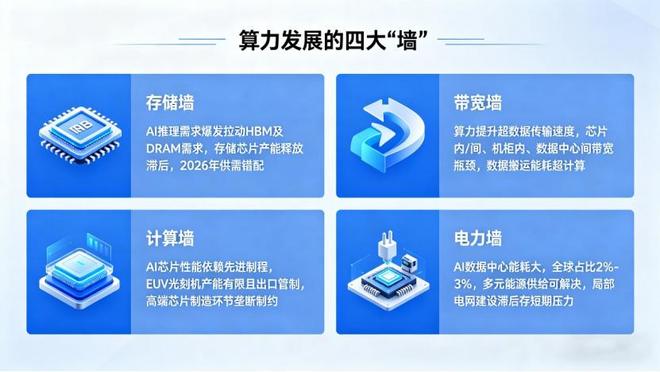
(1) Storage Wall: The First Shackle in the AI Inference Era
Currently, the AI industry's focus is shifting from large-scale model training to inference, with global AI inference demand expected to surpass training scenarios by 2026. The surge in AI inference-side demand directly drives the need for high-bandwidth memory (HBM) and large-capacity DRAM.
Although major memory chip manufacturers are planning to expand capacity, it takes at least two years from investment to actual production line launch, meaning the tight supply situation is unlikely to ease in the short term. New capacity will mainly come online in 2027 and beyond, resulting in a structural mismatch in 2026 where demand grows rapidly while supply lags.
(2) Bandwidth Wall: "Capillary Blockage" in Data Flow
The speed of computing power improvement far exceeds that of data transmission, leading to a severe "bandwidth wall" problem—data flow within chips, between chips, inside racks, and across data centers has become a performance bottleneck for the entire computing system.
The current bandwidth bottleneck is multi-layered: Inside chips, interconnect delays and power consumption between transistors continue to rise; between chips, traditional PCB-based interconnects can no longer meet the high-bandwidth, low-latency requirements of AI chips; inside racks, interconnect bandwidth between servers constrains scale-up (vertical scaling); between data centers, long-distance transmission bandwidth and latency limit scale-out (horizontal scaling) and cross-regional computing power scheduling efficiency.
It is estimated that in current AI training clusters, energy consumption from data movement already exceeds that of computation itself. How to unclog the "capillaries" of data flow and reduce transmission delays and power consumption is a problem that must be solved for AI Infra development.
(3) Computing Wall: High-End Chip Manufacturing as the Fundamental Constraint
AI chip performance iteration heavily relies on advanced process technology, whose capacity is entirely constrained by upstream high-end manufacturing equipment, especially EUV (extreme ultraviolet) lithography machines.
Currently, ASML is the only company globally capable of producing EUV lithography machines, with extremely limited capacity and subject to strict export controls. This directly results in a severe shortage of advanced process capacity below 7nm, unable to meet the explosive demand for AI chips. NVIDIA, the global leader in AI chips, has seen its shipments of high-end chips like the H100 and H200 constrained by TSMC's advanced process capacity, with lead times extending to several months or even over a year.
More critically, chip manufacturing is a highly globalized industry chain where disruptions in any link affect overall capacity. From raw materials like photoresist, target materials, and electronic specialty gases to key equipment like etchers and deposition tools, various degrees of monopoly and supply restrictions exist. This makes high-end chip manufacturing capacity the most difficult bottleneck to break through in the AI Infra industry chain.
(4) Power Wall: A Relatively Controllable Short-Term Challenge
Compared to the first three, the power wall is a relatively easier bottleneck to address. AI data centers are major energy consumers, with annual power consumption of a mega-scale data center campus even exceeding that of a medium-sized city with hundreds of thousands of people. Currently, global data center electricity consumption accounts for 2%–3% of total global electricity use and is still climbing. However, the power issue is essentially an infrastructure construction problem that can be solved through diversified energy supply methods such as gas turbines, fuel cells, and photovoltaics.
In the long term, with the development of renewable energy technologies and the improvement of energy infrastructure, power supply will not become the biggest mid-to-long-term bottleneck for AI computing power development. However, in some regions, short-term power supply pressures due to lagging grid construction may still limit data center construction speed.
02
The "Invisible Killer" of Expansion: Comprehensive Shortages of Equipment and Materials
AI chip expansion speed is far below expectations, with the core constraint not being the chips themselves but comprehensive shortages in upstream equipment and materials.
(1) Rapid Growth in Test Equipment Demand
Technological upgrades in AI chips have raised precision and efficiency requirements for test equipment. Compared to ordinary logic chips, AI GPUs have a massive increase in signal port count, consuming more signal channel resources from testers; simultaneously, the surge in transistor count has greatly increased test vector scale and per-chip testing time. More critically, while only a certain proportion of chips are tested in traditional consumer electronics, all AI chips must undergo 100% testing, often through multiple stages, to ensure the entire chipset functions properly. Driven by strong AI computing power demand and the explosion in the memory market, semiconductor test equipment (ATE) has become the fastest-growing category in the entire semiconductor equipment sector.
Advantest, the world's largest chip test equipment supplier, also stated that it expects to reach a record high in the fiscal year ending March 2026, with revenue projected to grow 37% and net profit more than doubling year-on-year.
(2) IC Substrate/Package Substrate: A More Expensive "Chokepoint" Than Chips
Surprisingly, the biggest supply chain pain point for leading chip manufacturers like NVIDIA is not the chips themselves but IC substrates (package substrates). IC substrates are key components connecting chips to PCBs, providing electrical connections and physical support. AI chips have extremely high requirements for IC substrates—requiring larger area, higher routing density, better heat dissipation performance, and lower signal loss. This also means their value is inevitably much higher than ordinary PCBs. It is estimated that IC substrate costs account for about 50% of total packaging costs, and in advanced flip-chip packaging, this proportion even reaches 70%–80%. Depending on the resin material selected, IC substrates are mainly divided into BT substrates and ABF substrates. BT substrates are primarily used for various memory chips, while ABF is more concentrated in logic chips such as CPUs, GPUs, FPGAs, and ASICs.
According to incomplete statistics, IC substrate prices have cumulatively risen by over 30% since 2025. The price hikes are mainly due to two reasons: First, cost pass-through from upstream raw materials, with core materials like high-end glass fiber cloth and copper foil in continuous short supply since 2025, widening the capacity gap; second, explosive demand from 2.5D/3D advanced packaging, with high-end chips like GPUs widely adopting multi-chip stacked architectures, significantly increasing chip layers and area, directly driving up substrate area demand.
Unlike ordinary PCBs, IC substrates have high technical barriers and complex processes, with global high-end IC substrate capacity concentrated in a few Taiwanese manufacturers like Unimicron and Nanya PCB, with capacity expansion cycles as long as 18–24 months. This means the tight supply situation for IC substrates is unlikely to be fundamentally resolved in the next two years.
(3) Key Specialty Materials: Extremely Scarce "Industrial MSG"
Some seemingly insignificant specialty materials are becoming the "fatal weakness" of the AI industry chain. Materials like Low-CTE (low coefficient of thermal expansion) glass fiber, specialty copper foil, and high-end drill bits, while used in small quantities, are indispensable "industrial MSG" for manufacturing high-end IC substrates and PCBs.
The high power consumption and performance requirements of AI chips necessitate the use of materials with extremely low thermal expansion coefficients for substrates and PCBs to prevent deformation under high-temperature operating environments. Meanwhile, as fillers harden, the lifespan of drill bits used in processing shortens dramatically to 1/5–1/7 of the original, leading to explosive growth in drill bit demand.
These specialty materials have extremely high technical barriers, with global capacity highly concentrated and expansion difficulties. Any supply disruption will directly impact the normal operation of the entire AI industry chain.
(4) High-End Cleanrooms: A Neglected High-Barrier Segment
In the expansion of the AI industry chain, high-end cleanrooms are another severely overlooked high-barrier segment. Advanced process chips and advanced packaging have extremely high cleanliness requirements for production environments, where a single dust particle in the air can cause an entire wafer to be scrapped.
The construction of high-end cleanrooms requires not only massive capital investment but also extremely high technical levels. From air purification systems to anti-static facilities, from temperature and humidity control to vibration isolation, every link has strict standards. Currently, the global high-end cleanroom market is mainly dominated by overseas manufacturers, with net profit margins exceeding 20%, much higher than domestic peers.
With the global expansion of AI chip capacity, demand for high-end cleanrooms remains strong, making it a highly certain and prosperous segment in the industry chain.
03
The "Route Battle" of Connection Technologies: Copper Resurgence and Optoelectronic Fusion
Beyond computing power and expansion bottlenecks, connection technologies within data centers are undergoing profound transformations. The technological route battle between copper and light, along with PCB/substrate technological upgrades, is reshaping the AI Infra connection landscape.
(1) Scenario-Based Competition and Substitution Between Copper and Light
For a long time, optical modules have been considered the future direction for high-speed interconnects in data centers. However, with the explosion in AI computing power demand, copper cable technology is experiencing a "resurgence," with copper and light forming complementary and substitutable relationships in different scenarios.
Short distances (≤7 meters): Copper cables (AEC, active copper cables) are comprehensively replacing laser-based optical modules due to their low cost, high reliability, and low latency advantages. In short-distance interconnect scenarios inside servers and racks, copper cables offer clear cost-performance advantages.
Medium distances (~30 meters): Micro LED optical cables have become a compromise solution. Combining the advantages of copper cables and optical modules, they offer better reliability than laser optical modules and lower costs than traditional optical modules, suitable for medium-distance interconnects between racks.
Long distances (between data centers): Traditional pluggable optical modules and fiber optics remain the mainstream. CPO (co-packaged optics) technology is considered the future direction, integrating optical engines with chips to significantly boost bandwidth and reduce power consumption. However, it still faces challenges like high costs and poor reliability, with large-scale commercialization still some time away.
Notably, the procurement scale and performance specifications for optical fibers in AI data centers have created a magnitude gap compared to traditional telecom networks. To meet the low-latency, high-bandwidth interconnect requirements of GPU clusters, demand for specialty optical fibers like G.657.A2 continues to rise, while more cutting-edge hollow-core fiber solutions have entered actual deployment stages. Hollow-core fibers replace traditional glass cores with air, significantly optimizing transmission performance: transmission loss can be reduced from conventional 0.14 dB/km to below 0.1 dB/km, transmission delay from 5 μs/km to 3.46 μs/km, while tolerating higher optical power.
Currently, the number of manufacturers participating in the hollow-core fiber market is rapidly expanding, yet prices remain relatively stable at around 30,000–40,000 yuan/km, much higher than ordinary optical fibers.
(2) Technological Upgrade Pressures on PCB/Substrates
To meet the high-bandwidth requirements of AI chips, PCB and substrate technologies are continuously upgrading. Currently, PCB/substrates are evolving toward n+m structures, glass substrates, and modified semi-additive process (mSAP) technologies.
The n+m structure enhances substrate bandwidth capacity by increasing layer count and routing density; glass substrates, with their lower thermal expansion coefficients and better high-frequency performance, are an important development direction for future high-end substrates; the mSAP process enables finer circuit routing to meet high-density interconnect demands.
These technological upgrades place new requirements on upstream equipment, materials, and manufacturing processes, bringing new industrial opportunities and challenges.
04
Conclusion
The AI Infra industry chain is facing intertwined multi-dimensional bottlenecks. From the storage wall, bandwidth wall, computing wall, and power wall at the computing power level, to shortages in test equipment, IC substrates, specialty materials, and cleanrooms at the expansion level, to the technological route battle at the connection level, every link affects the large-scale deployment of AI computing power.
High-end chip manufacturing capacity is the most fundamental constraint, determining the performance upper limit and capacity scale of AI chips. Meanwhile, test equipment, high-end IC substrates, and key specialty materials represent the segments with the strongest certainty and most prominent supply-demand contradictions in the current industry chain. In the long term, AI Infra development will present two major trends: First, the technological evolution of copper resurgence and optoelectronic fusion, with different technological routes coexisting in their respective advantage scenarios; second, the restructuring of the global industry chain and accelerated localization, with domestic enterprises expected to achieve breakthroughs in some niche segments.
-
![]()
Tesla Restructures Its Balance Sheet
-
![]()
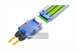
Accelerating the High-Speed Interconnection Upgrade of AI Computing Clusters! JONHON Releases ELSFP External Light Source Optical Connectors
-
![]()
Breaking the overseas blockade of volumetric holographic materials, this optical enterprise secures nearly 100 million yuan in financing!
-
![]()
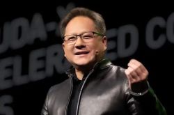
Why Does Jensen Huang So Openly Praise China’s AI?
-
![]()
"Wudang" Unveiled: Arm China's Next-Gen AI VPU Redefines Video Encoding
-
![]()
From Energy Conservation and Carbon Reduction to AI Decision-Making: GECON East Intelligence and Chery Group Explore a New Green and Smart Paradigm for Automobile Manufacturing
-
![]()
WAIC 2026 Observation | AI Accelerates Towards the Core of Industries, Industrial AI Enters a Critical Phase
-
![]()
Volkswagen China Fires the First Shot in Foreign-Funded 'White Box Delivery'!