800 Trillion Won Bet: Samsung and SK Hynix to Build Two Wafer Fabs Each
 06/29 2026
 562
562
On June 29, Jung Gwan Kim, Minister of Trade, Industry and Energy of South Korea, announced that the country would concentrate on building four semiconductor wafer fabs in the southwest region, with Samsung Electronics and SK Hynix each undertaking the construction of two fabs, at a total investment of approximately 800 trillion won. The announcement immediately drew widespread attention in the industry on the day of its release. 800 trillion won is equivalent to approximately RMB 4 trillion, exceeding one-third of South Korea's 2024 GDP.
The investment structure primarily involves the southwest region of South Korea taking on wafer manufacturing capacity, the central region focusing on advanced packaging, and the southeast region developing a complete industrial chain for materials, components, equipment, and next-generation power semiconductors. The three regions have clear divisions of labor and mutually support each other, forming a vertically integrated layout from front-end to back-end processes, and from manufacturing to materials.
Additionally, in terms of research and development, the South Korean government plans to invest 30 trillion won over the next 15 years specifically for the development of next-generation memory technologies. Priority areas include the iterative development of subsequent HBM specifications and new types of non-volatile memory technologies. Meanwhile, the government has committed to accelerating the project approval process and expediting the construction of supporting infrastructure to release actual production capacity as soon as possible.
At the press conference, Jung Gwan Kim cited a set of forecast data indicating that the global market size for memory chips is expected to grow to four times its current level over the next five years. Behind this forecast is the structural expansion of demand for high-bandwidth memory from AI servers, edge computing devices, and automotive electronics.
Industry insiders believe that South Korea's decision to lock in investment at this juncture is partly driven by the desire to seize the production capacity window before the large-scale release of AI memory demand.
However, from a broader perspective, the significance of this plan extends beyond mere capacity expansion. To a considerable extent, it represents an active reshaping of the current competitive landscape in the memory industry. South Korea aims to extend its technological generational advantage in the industry through large-scale, government-led collaborative investments.
Whether this integration can be implemented as planned still depends on whether the capital expenditure intention (willingness) of the two companies aligns with the pace of global demand.
-
![]()
The Unstoppable Rise of 'Optical Progress and Copper Decline': Sunny Optical’s Strategic Vision for the Next Decade
-
![]()
AI + Going Global in the Second Half: No Intermission for Robot Vacuum Cleaners
-
![]()
The Suffering Endured in E-commerce, Walmart Doesn't Want to Repeat in AI
-
![]()
What Does the Doubling of New Energy Vehicle Exports Mean?
-
![]()
Ghosn: 'Only I Can Save Nissan'
-
![]()
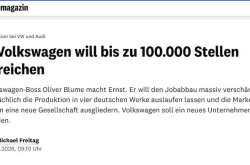
Volkswagen Lays Off 100,000 Employees, The Elephant Sits Down
-
![]()
Expanding Production Capacity! Yutong Optics Acquires Approximately 1.5 Hectares of Industrial Land in Chang'an, Dongguan
-
![]()
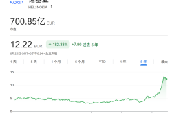
Why Is Nokia Making a Comeback in the AI Era?